Flash Memory Summit 2018, Yangtze Memory Technology Keynote Live Blog: Unleashing 3D NAND
by Ian Cutress & Billy Tallis on August 7, 2018 5:50 PM EST
05:53PM EDT - The final talk of this session is from Yangtze Memory Technology (YMTC). We published their announcement this week, but they have set a very interesting talk for the show. The talk is called 'Unleasing 3D NAND's Potential with an Innovative Architecture'.
05:54PM EDT - Set to start in 10 minutes!
05:55PM EDT - Here is our news from earlier in the week:
05:55PM EDT - https://www.anandtech.com/show/13166/yangtze-memory-unveils-xtacking-architecture-for-3d-nand-up-to-3-gbps-io
05:57PM EDT - YMTC is a newcomer to FMS, and they seem to have grabbed Samsung's vacated time slot
06:03PM EDT - OK here we go
06:03PM EDT - Simon Yang to the stage
06:03PM EDT - CEO
06:04PM EDT - 'We're a new kid in the neighbourhood'
06:04PM EDT - Usually Yang is at IEDM
06:04PM EDT - A couple of years ago, he knew next to nothing about NAND
06:05PM EDT - 'we are a bunch of good kids
06:05PM EDT - Make a contribution to the industry
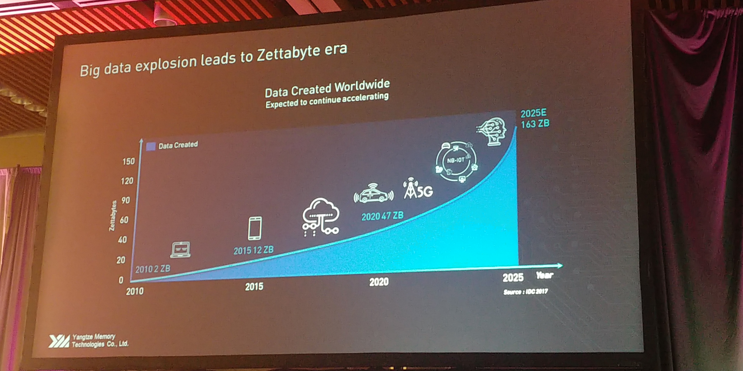
06:06PM EDT - Expected 163 ZB Big Data explosion by 20205
06:06PM EDT - Most data is garbage
06:06PM EDT - But our habit is to store data
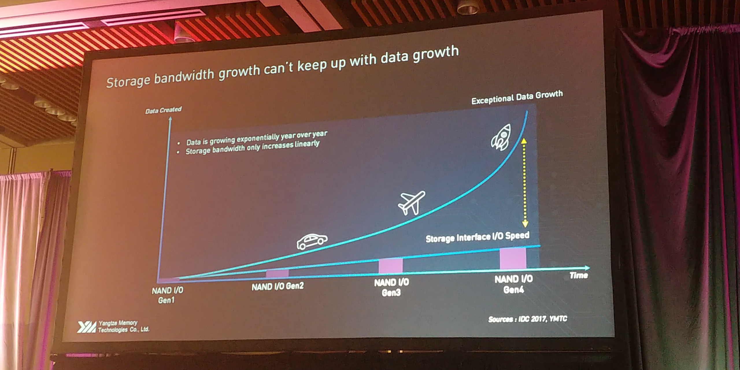
06:07PM EDT - Data speed only increasing linearly, but data created is exponential
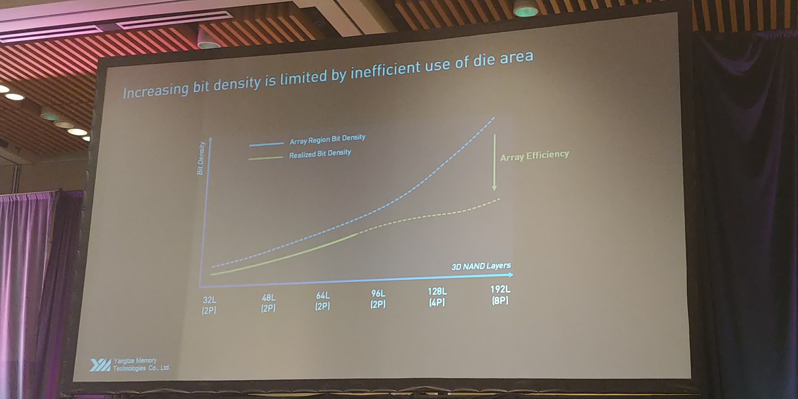
06:07PM EDT - Challenges of NAND: I/O speed, bit density, and time to market
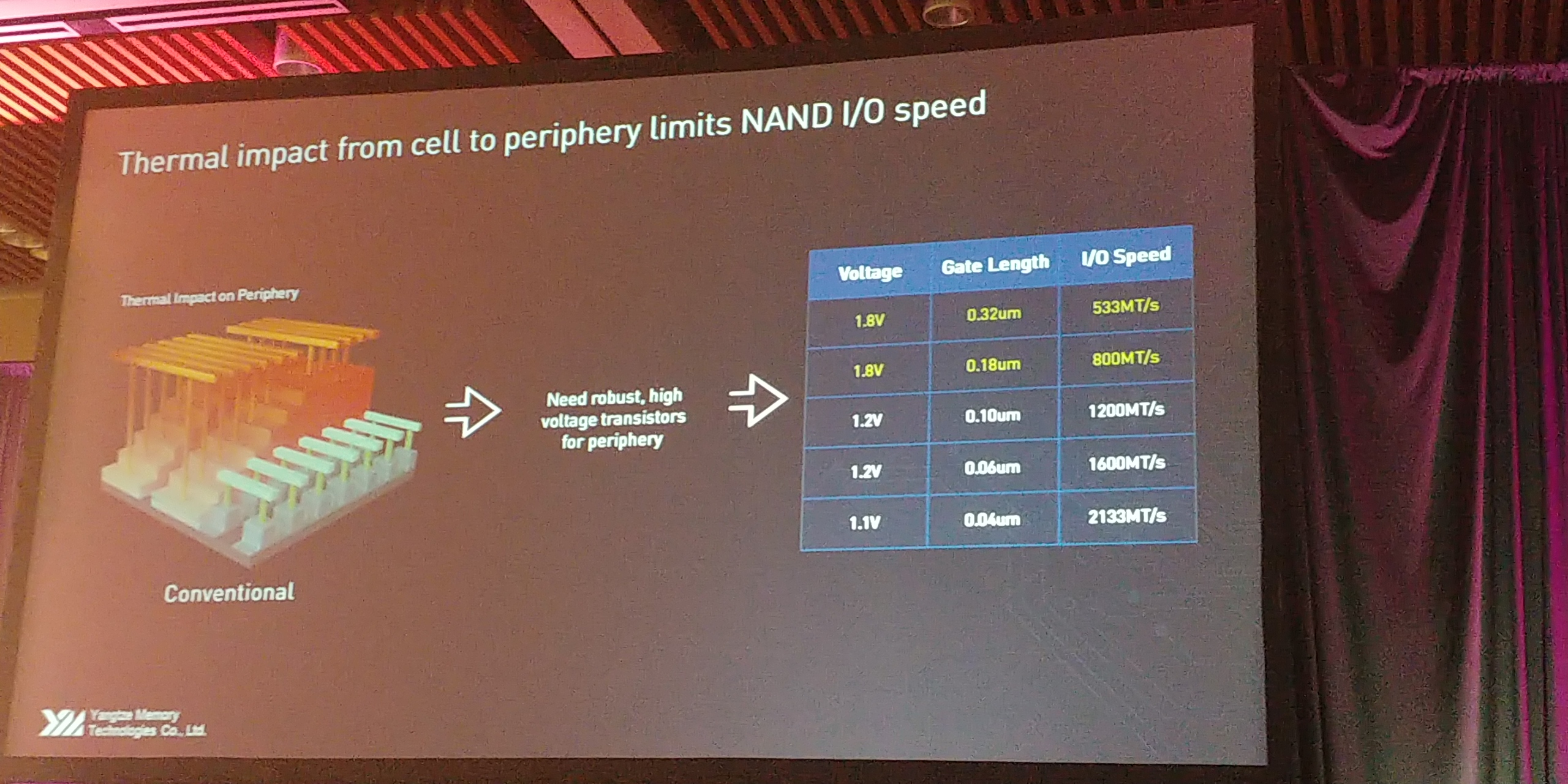
06:09PM EDT - Thermal impact limits the scaling and speed of NAND
06:09PM EDT - High thermal process prevents scaling of process
06:09PM EDT - (They just turned the lights on, so can't get good photos)
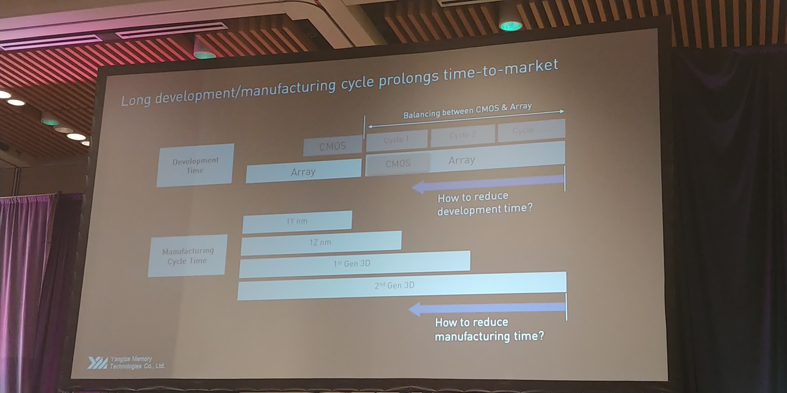
06:10PM EDT - Manufacturing cycle times have been getting longer
06:10PM EDT - YMTC aim to solve these problems
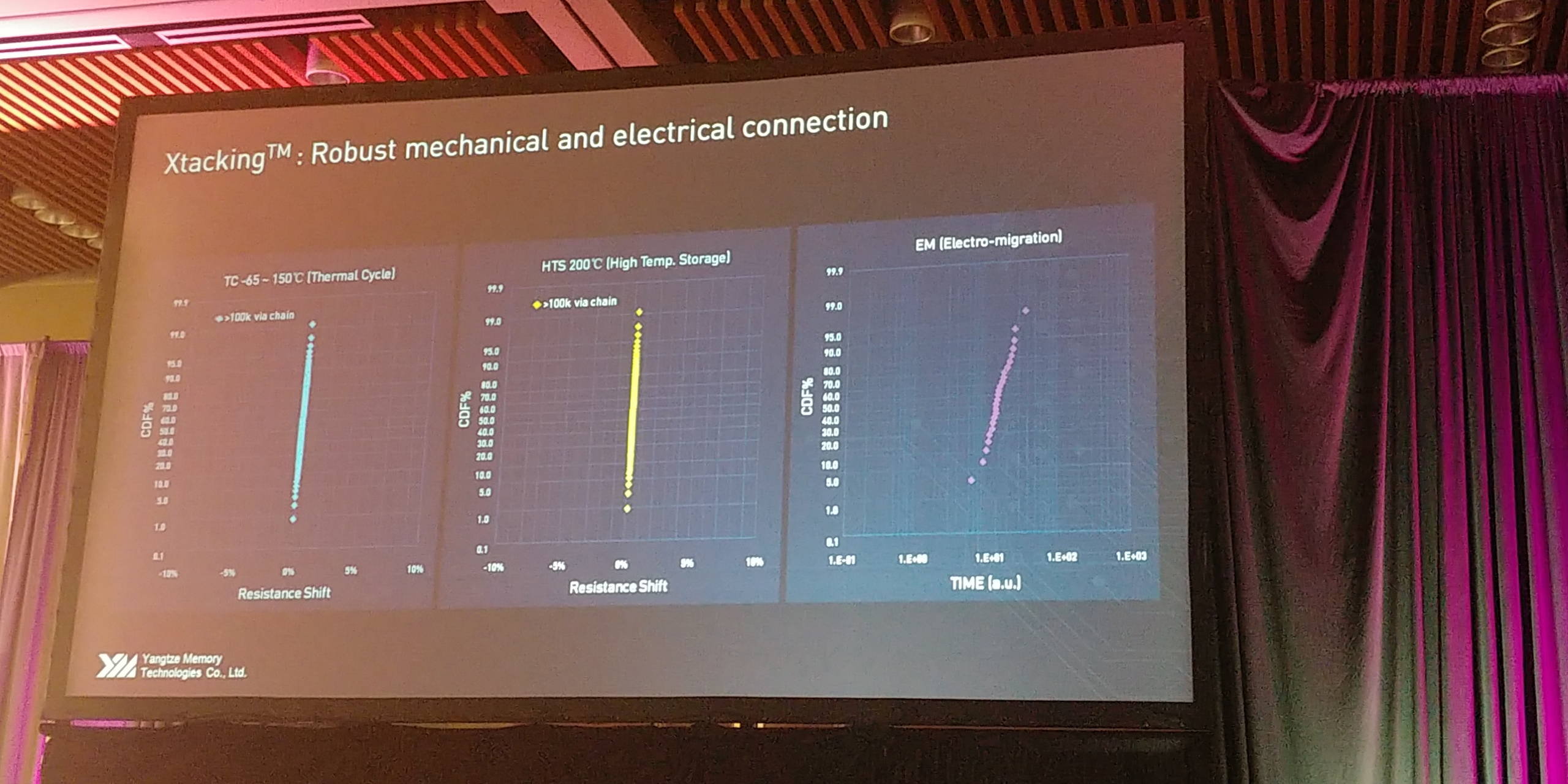
06:10PM EDT - Solution is Xtacking
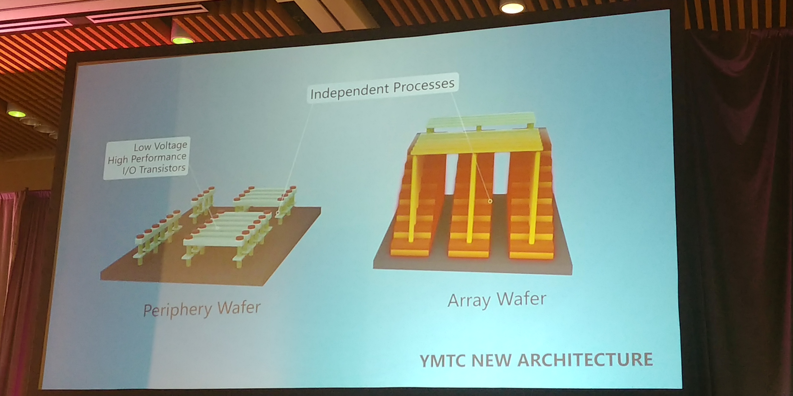
06:11PM EDT - Using low voltage periphery transistors and stacking allows for faster IO
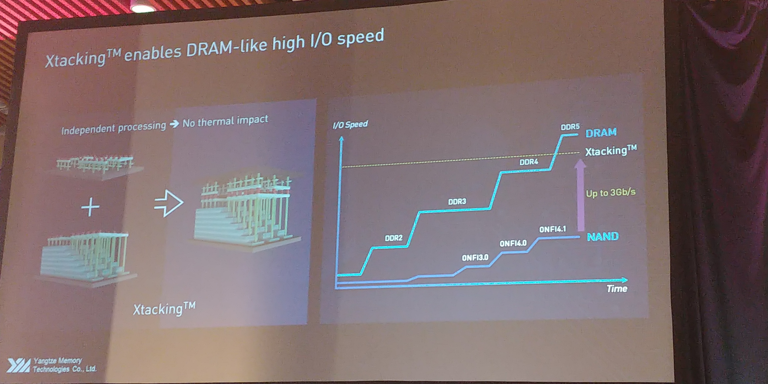
06:12PM EDT - Moves IO speed up to DDR speeds
06:12PM EDT - Up to 3 Gbps IO
06:12PM EDT - Use up to 14nm to boost IO speed

06:12PM EDT - Putting the periphery above the stack

06:13PM EDT - YMTC proposes 3Gbps wheil Samsung and SK Hynix are talking 1.4Gbps and 1.2Gbps
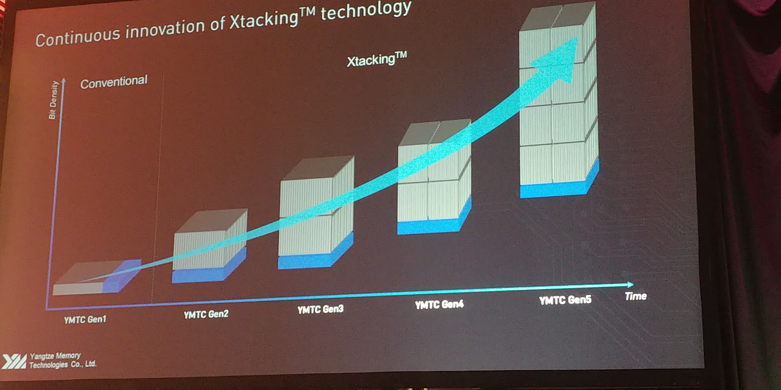
06:13PM EDT - Bit density on YMTC 64-layer only 10-20% below 96 layer
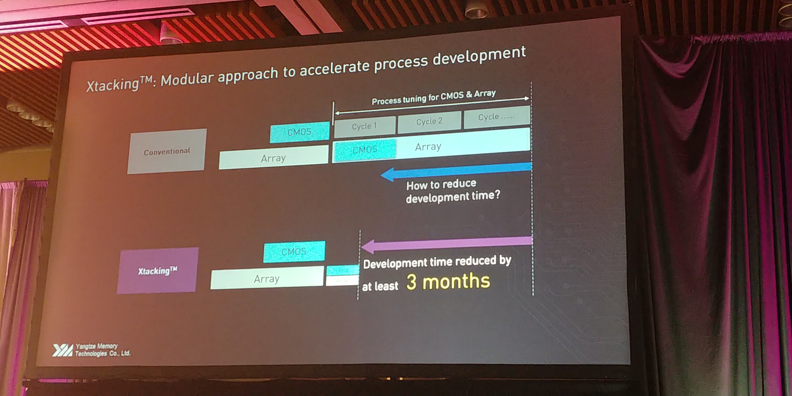
06:14PM EDT - reducing time to market by 3 months
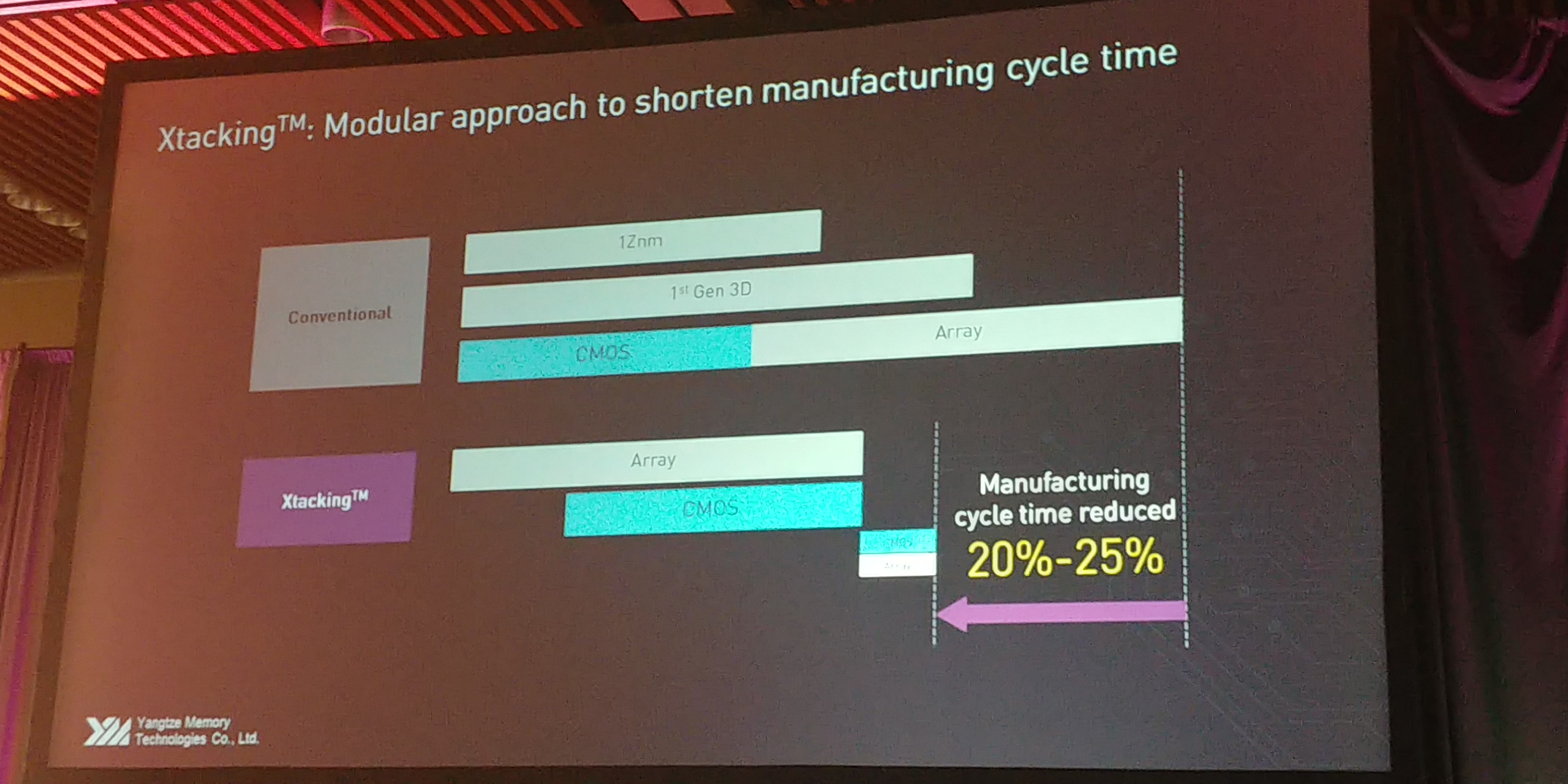
06:14PM EDT - develop wafers differently means can work on independently, and shorten manufacturing cycle time by 20-25%
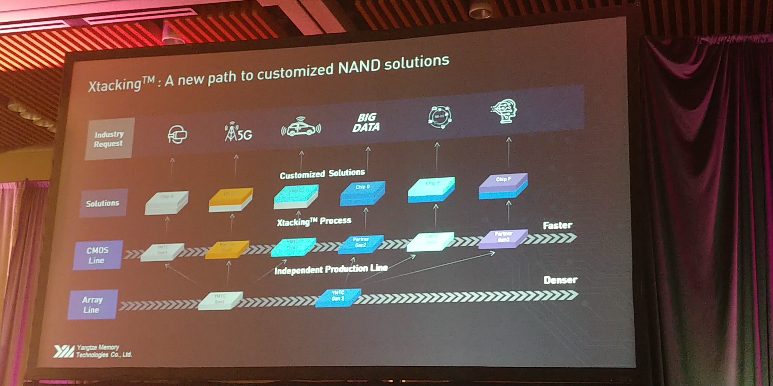
06:14PM EDT - Also allows for customized designs for each market
06:15PM EDT - Use different peripheral logic for each customer
06:15PM EDT - Allowing customers to win
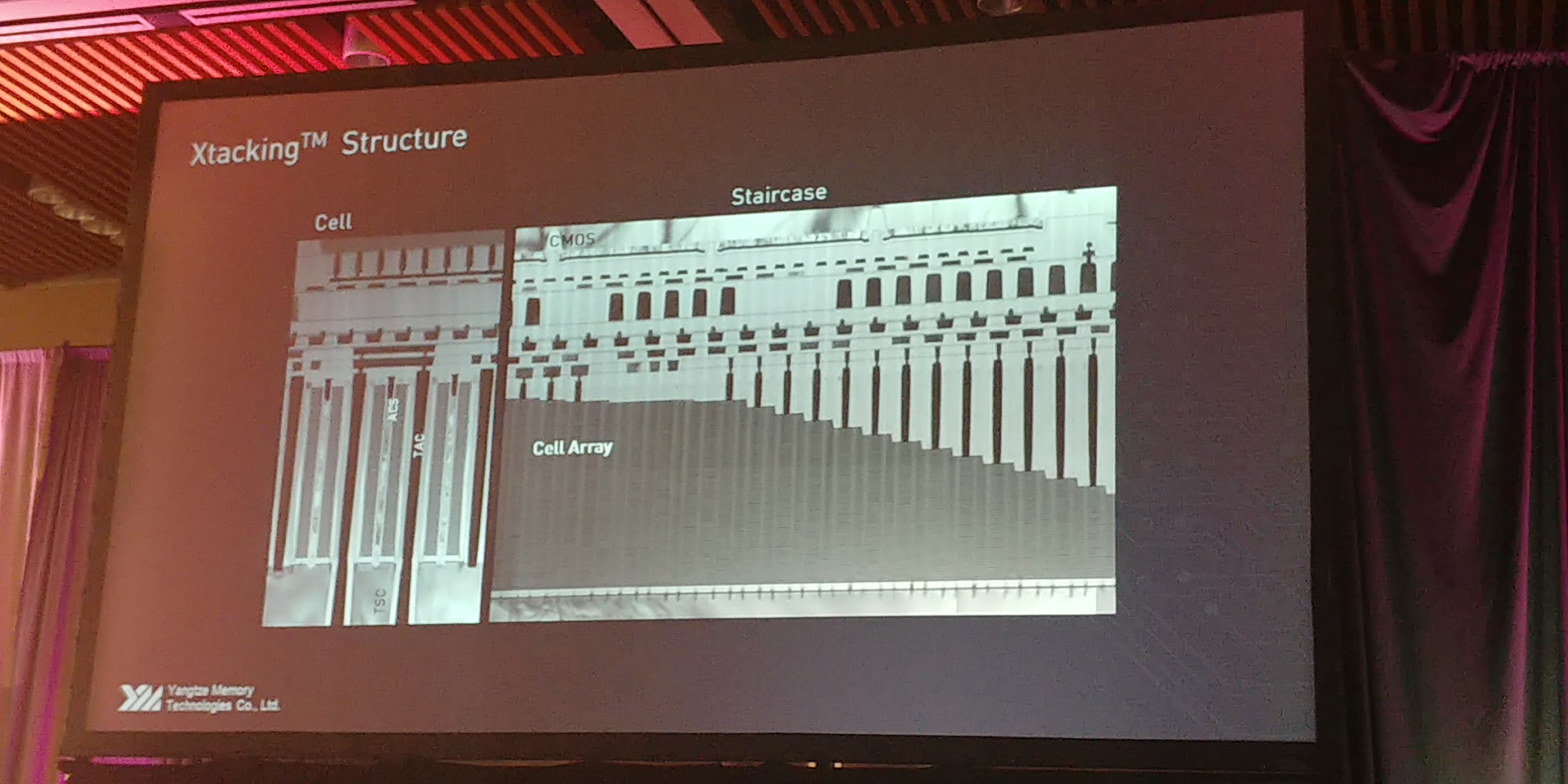
06:15PM EDT - Cells and staircase structure
06:16PM EDT - Pushing the technology into low nanometer generations
06:16PM EDT - Re-engineering the interface material
06:16PM EDT - Re-engineering based on design rules for each wafer
06:16PM EDT - Develop own slurry to enable the technology
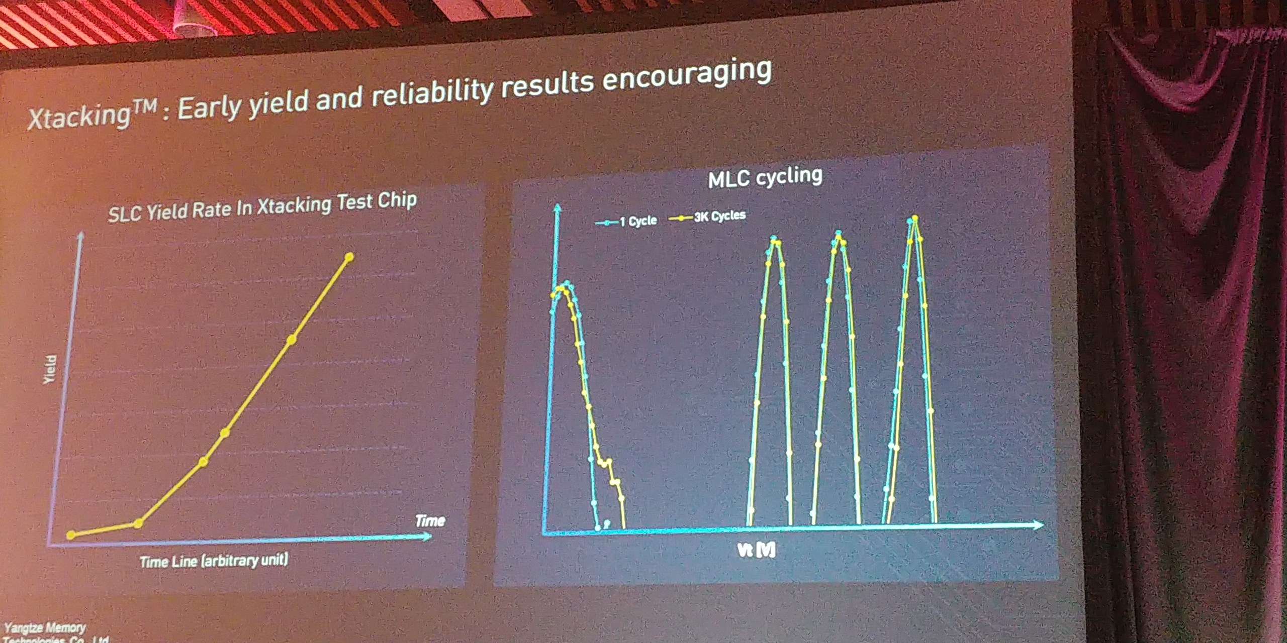
06:17PM EDT - SLC yield rate is increasing, MLC cycling is getting better
06:17PM EDT - Yield is not Xtacking limited
06:17PM EDT - Working on multiple generations simultaneously
06:18PM EDT - YMTC wants to contribute to the industry
06:18PM EDT - The main question is where di YMTC come from
06:18PM EDT - Story time
06:18PM EDT - Yang previously worked for Intel
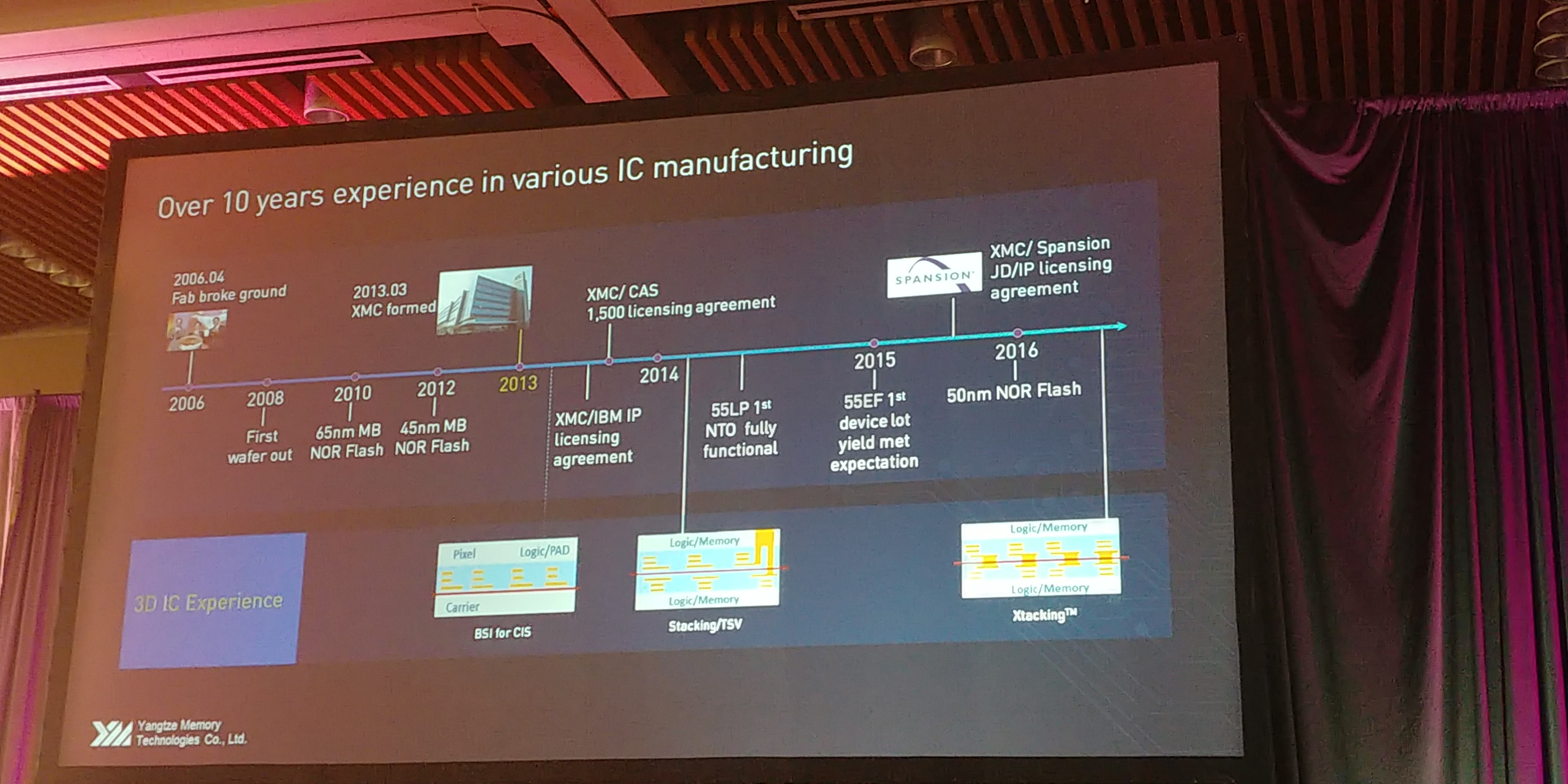
06:19PM EDT - Then toured around the world, then worked for 12-inch fab in 2012
06:19PM EDT - Ended up in XMC
06:19PM EDT - This is where Xtacking happens
06:19PM EDT - Mainly NOR up to now
06:20PM EDT - 2015, signed joint 3D NAND agreement with Spansion
06:20PM EDT - Working on wafer level stacking technology
06:20PM EDT - 3D NAND R&D started in 2014
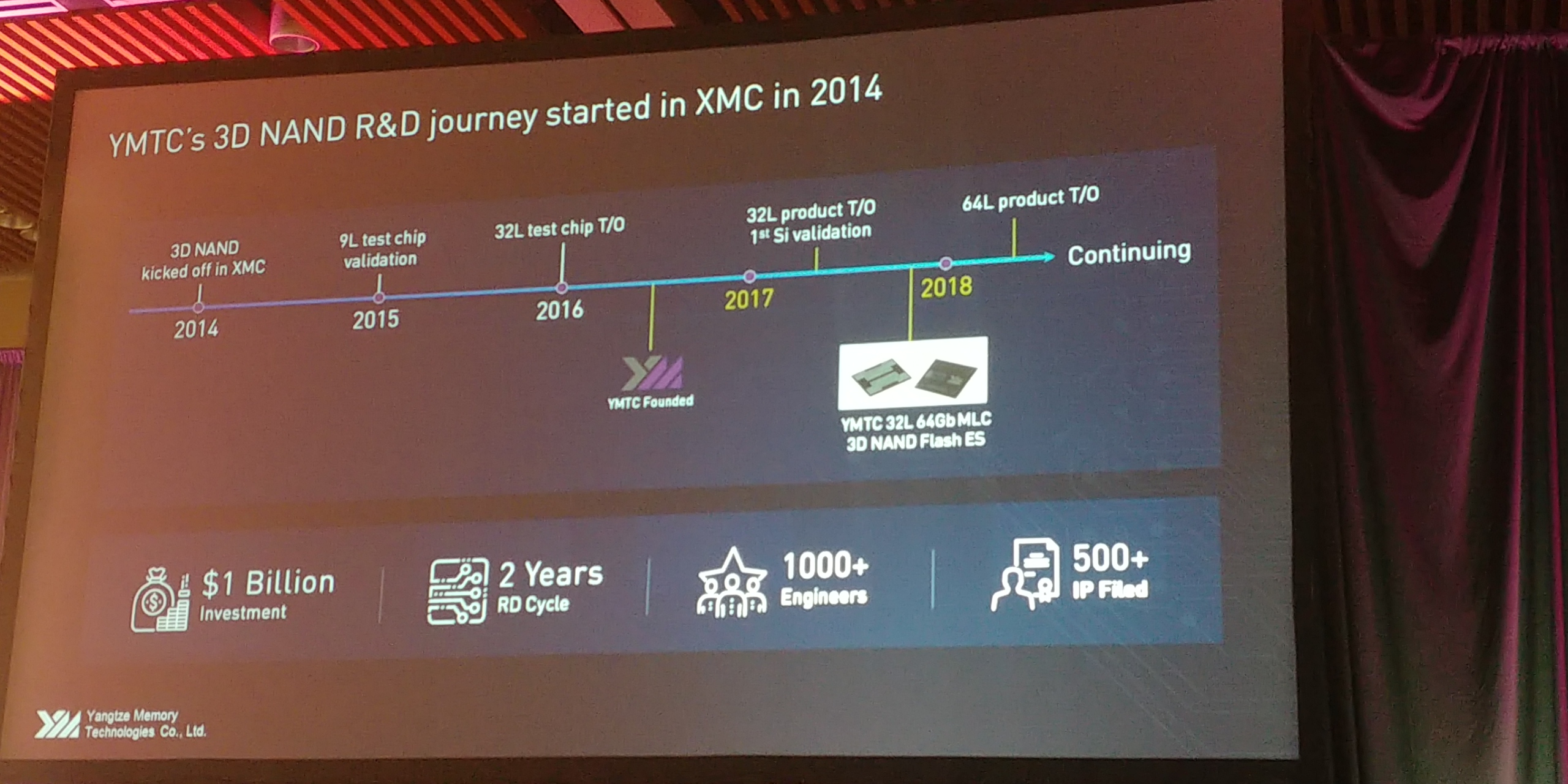
06:21PM EDT - $1B development in 3D NAND
06:21PM EDT - YMTC founded in 2016
06:21PM EDT - YMTC founded in 2016
06:21PM EDT - hiring lots of people to catch up to incumbants
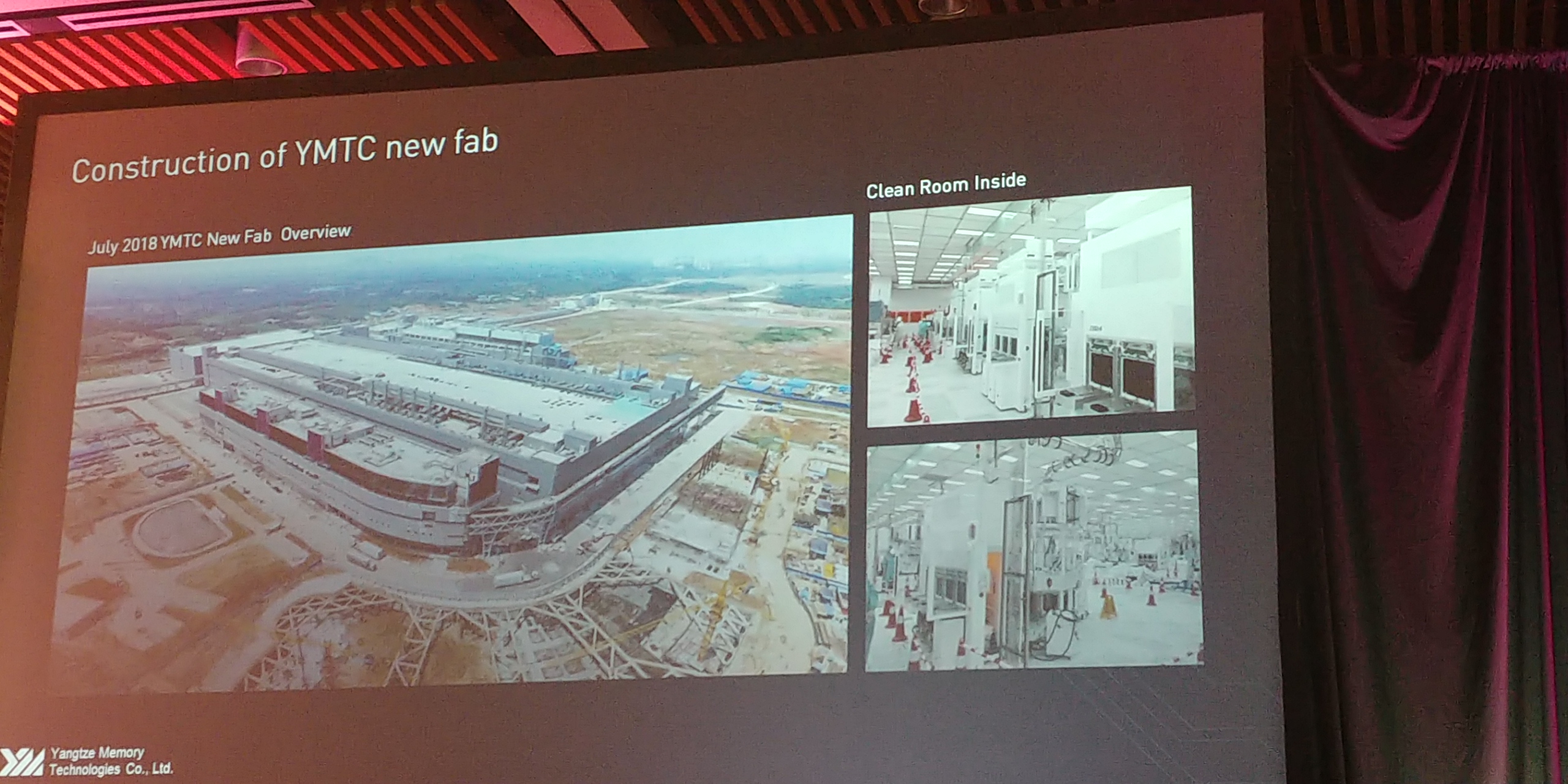
06:22PM EDT - Fab is 60-70k sq m
06:22PM EDT - First gen product currently made in small fab
06:22PM EDT - New fab will mainly be focused on the next generations
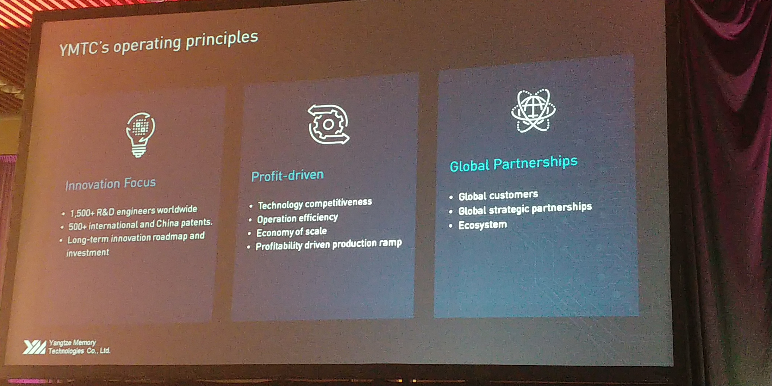
06:23PM EDT - YMTC is a group with pretty good tech capability for development
06:23PM EDT - Not afraid to go down new paths
06:23PM EDT - Follow market rule, and very much profit driven
06:23PM EDT - First gen product is already in very high yield
06:23PM EDT - But not in volume ramp, because from cost perspective it is not competitive
06:24PM EDT - Only want to ramp when it is cost competitive
06:24PM EDT - Very open for collaboration
06:24PM EDT - (most other 32L 3D NAND designs were also not very cost competitive)
06:24PM EDT - Want to serve the whole global market
06:24PM EDT - That's a wrap. Interesting stuff. Now meetings for the rest of the day


5 Comments
View All Comments
Tyns - Wednesday, August 8, 2018 - link
So they have this breakthrough tech that puts cmos under the array using two wafers (IMFT did that with one wafer) that decreases time to market and cost even though its doubling(?) wafers (during an ongoing wafer shortage) and will more than double the IO speed of the most performant competitors’ products......but they’re open to collaboration instead of crushing their competitors...
Hahahahahahah
Oh, I forgot their 64L is almost as dense as competitors’ 96L, ignore that they’re not ramping any NAND yet since none of it is cost competitive.
The Chinese memory industry is as yet a joke.
OwCH - Friday, August 10, 2018 - link
Well, the major improvement is that they can choose whatever node suits their needs best for each part. For NAND-cells, smaller isn't always better, as we saw a few years ago. For the peripheral parts, smaller will nearly always be better.On paper, the concept is rational and would definitely lead to better performance. The question is if they can produce real world results.
They are probably open for collab because their NAND-cell tech is way behind other manufacturers.
Nyte7 - Monday, August 13, 2018 - link
lol wow someone didn't get laid last night. Did a Chinaman get a promotion over you or something lol?jjj - Wednesday, August 8, 2018 - link
Wish the part on staircase optimization had more details and clarity.linuxgeex - Saturday, November 9, 2019 - link
"06:12PM EDT - Putting the periphery above the stack"Oops, you mean below.