MRAM Developer Day, GlobalFoundries Keynote Live Blog
by Ian Cutress on August 6, 2018 12:37 PM EST
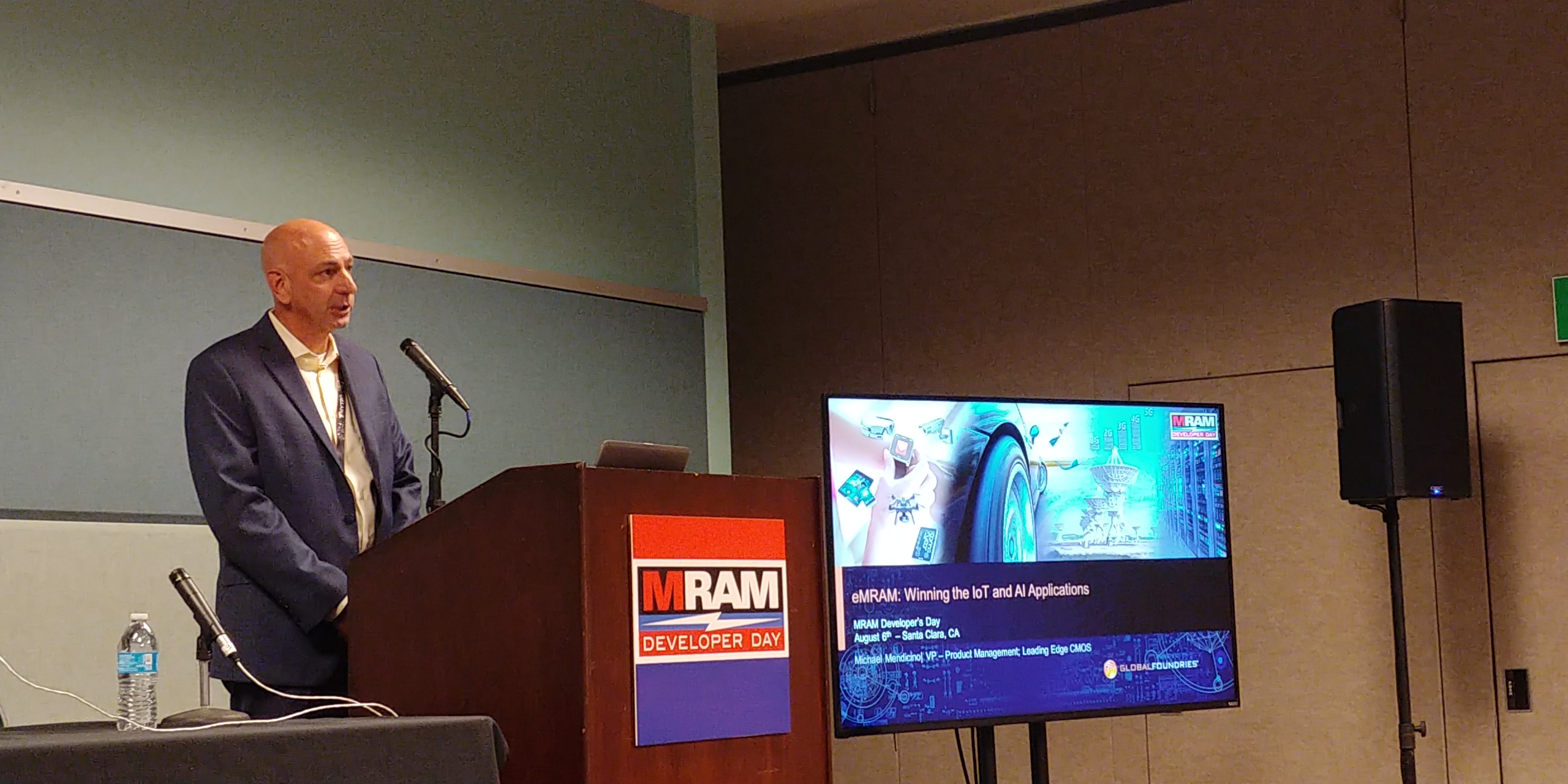
12:40PM EDT - Second Keynote today is from GlobalFoundries, Everspin's MRAM partner.
12:40PM EDT - Michael Mendicinoj, VP on stage
12:41PM EDT - 7% memory growth rate
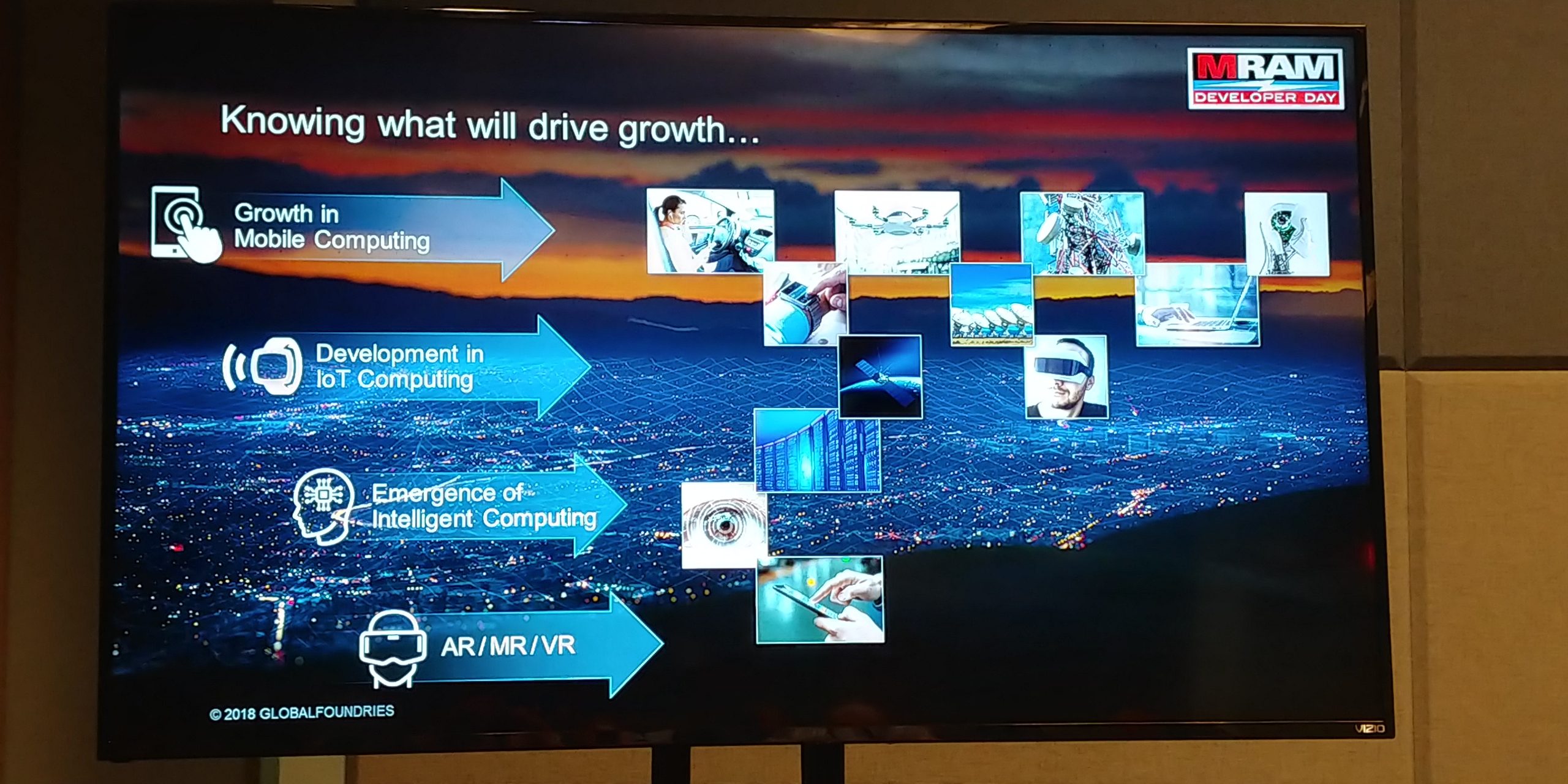
12:41PM EDT - Growth comes from many areas - mobile computing, IoT, AI, AR/MR/VR
12:42PM EDT - The key is to know what will drive growth and what will need it
12:42PM EDT - GF has a dual lane roadmap to tackle high performance and low power
12:42PM EDT - anticipating what the segments need from a total perspective
12:42PM EDT - Today is mostly IoT and AI related
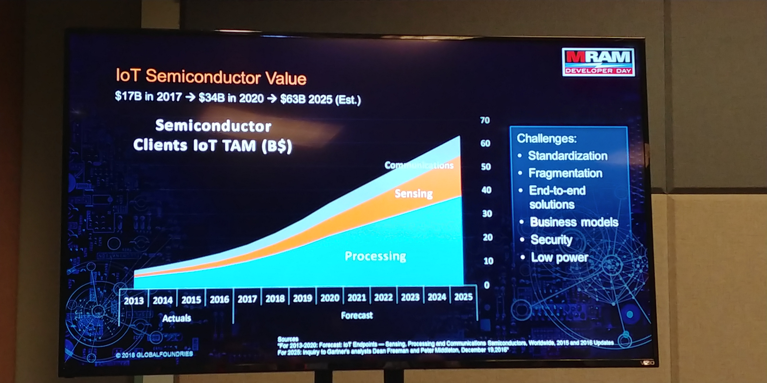
12:43PM EDT - Potential $63B TAM in 2025
12:43PM EDT - Connectivity is a big role in each space
12:43PM EDT - IoT is a very broad set of applications
12:43PM EDT - End-to-end solutions are important
12:43PM EDT - Needing to have the right capability in the technololgy
12:44PM EDT - Have a good overall cost of ownership

12:44PM EDT - IoT is not a segment - it's a collection of applications spread across segments
12:45PM EDT - Mobile Segment, Compute Segment, Automotive Segment, Aerospace segment
12:45PM EDT - Low power in 40-130nm, Mid range in 22-28nm, High perf at 12-14nm
12:46PM EDT - Speed and memory types vary
12:46PM EDT - RF is important across all segments
12:46PM EDT - 17 levels of metal at 7nm
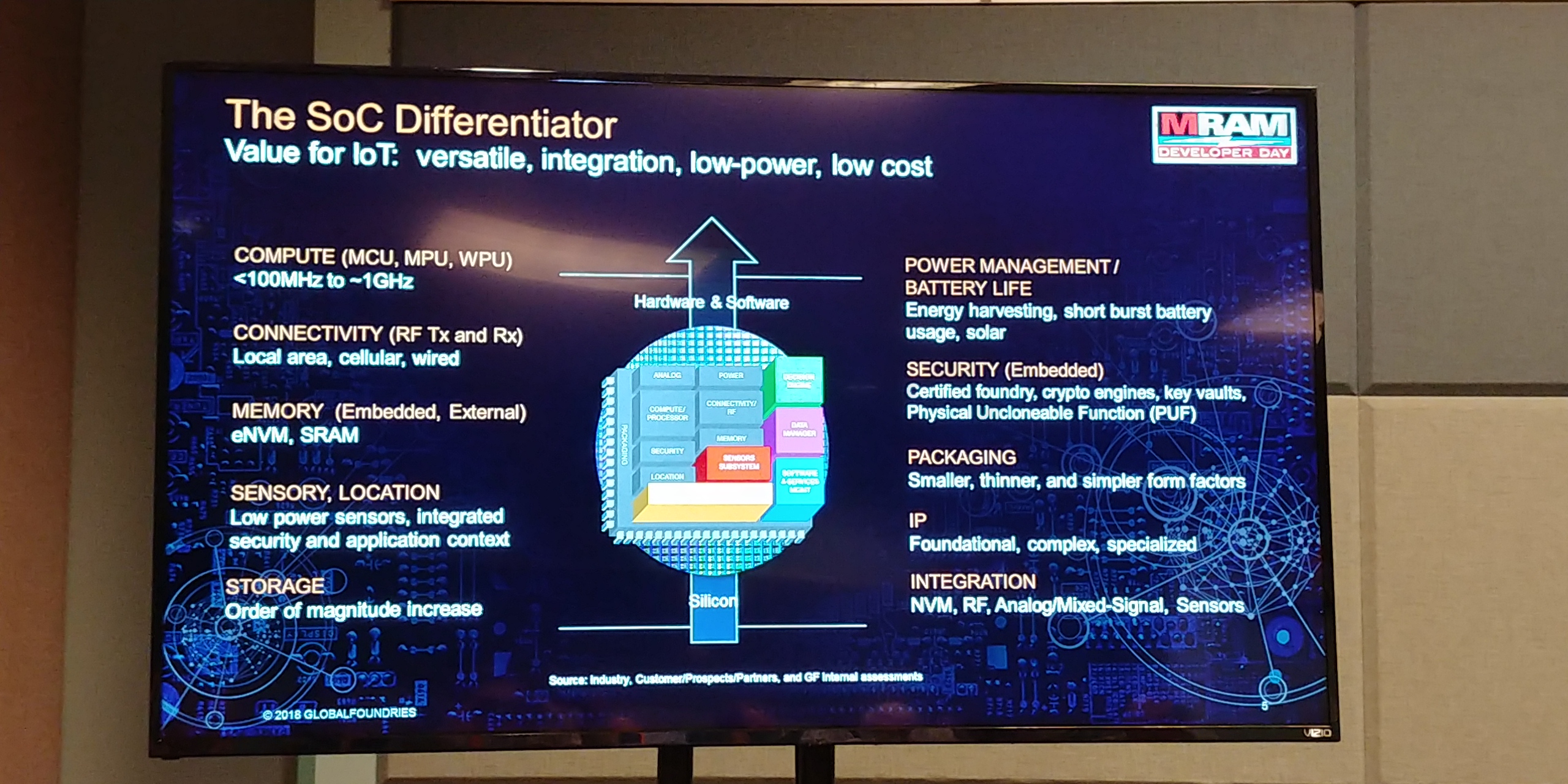
12:47PM EDT - The SoC Differentiator - to build value
12:47PM EDT - Some characteristics matter more depending on the IoT device
12:48PM EDT - Perf, Connectivity, Memory, Sensory, Storage, Battery, Security, Packaging, IP, Integration
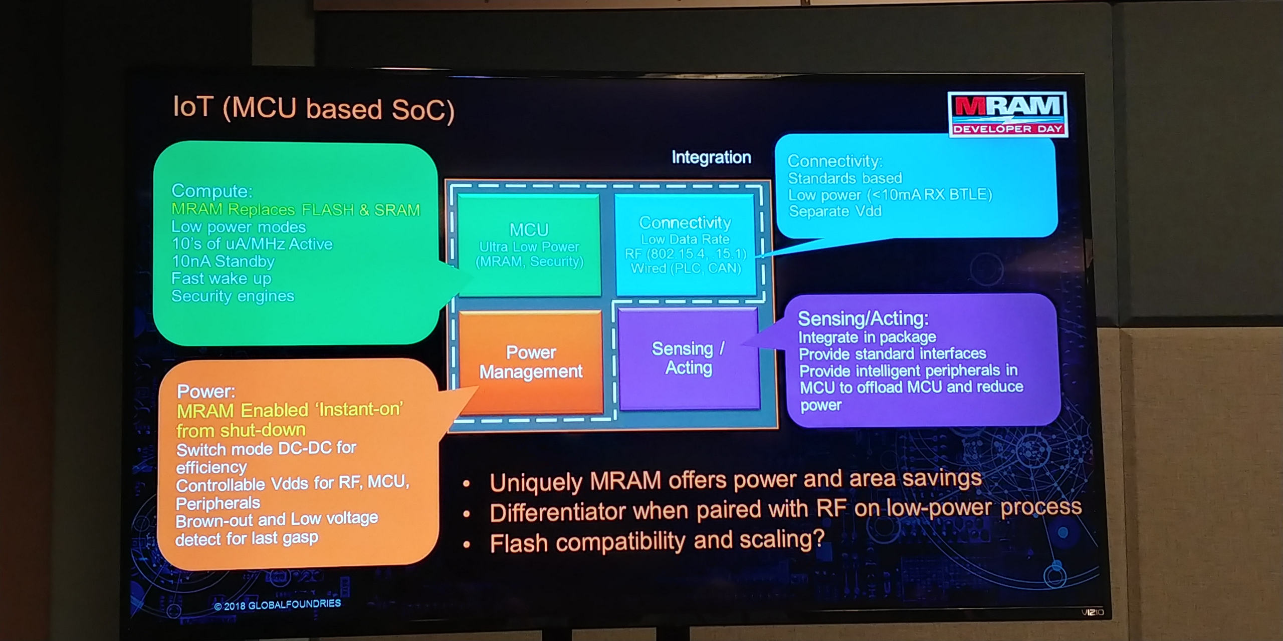
12:50PM EDT - MRAM offers power and area savings
12:50PM EDT - Instant On for IoT is important
12:51PM EDT - If you put good MRAM on a mediocre platform, that's not going to win
12:51PM EDT - Need best in class compute and RF to get max benefit
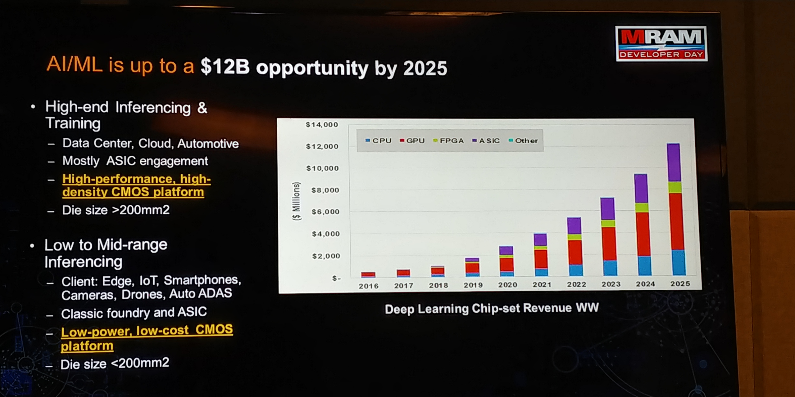
12:52PM EDT - AI is a key part of the semiconductor 7% CAGR
12:52PM EDT - Break it up into two main areas : Datacenter (high-end training and inferencing)
12:53PM EDT - These use the high end processes, big chips, mostly ASICs
12:53PM EDT - The other side is mid-to-low end inferencing: IoT, Smartphones, Drones, ADAS
12:53PM EDT - classic foundry and ASIC, smaller die size
12:53PM EDT - balanced low power process
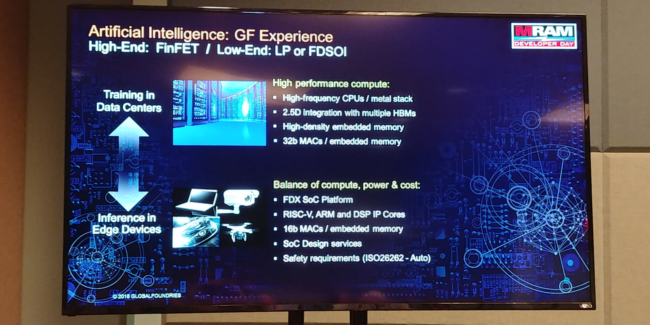
12:54PM EDT - IN high-end, big metal stacks requiremed, high density memory
12:55PM EDT - In edge devices, use FDX SoC platform, SoC design services
12:56PM EDT - Datacenter is usually based on thermal limits, low end is usually power limit driven
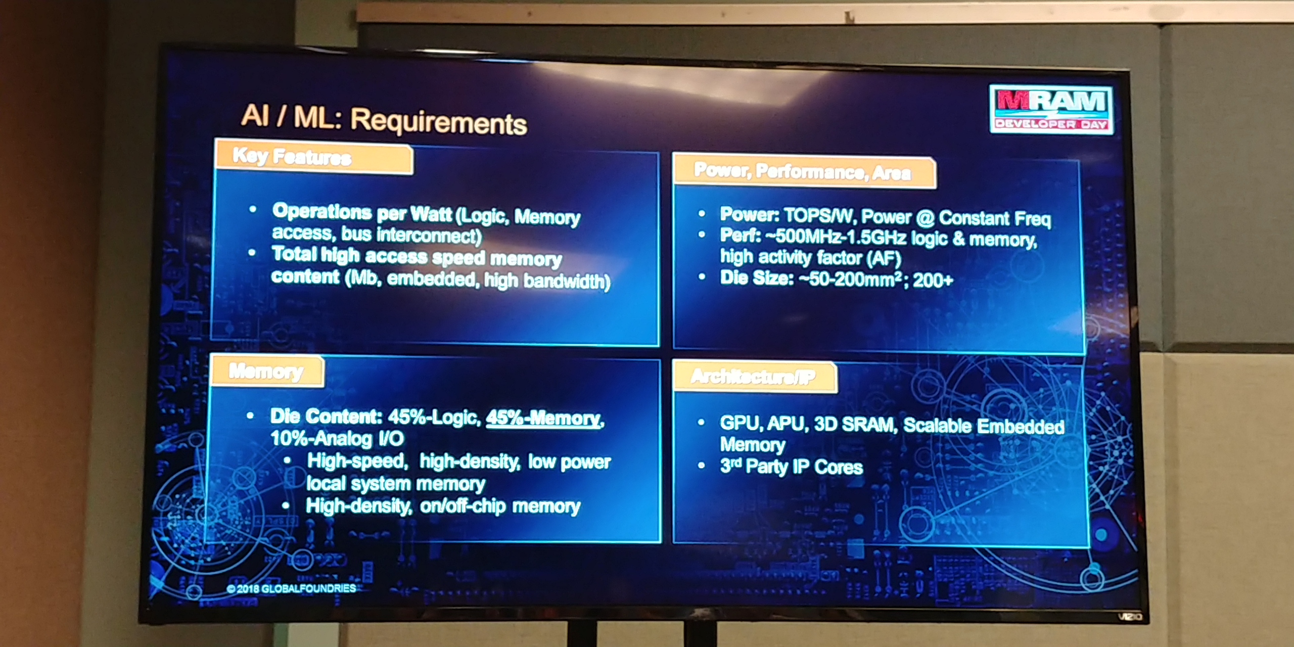
12:57PM EDT - How to win: IoT and ML
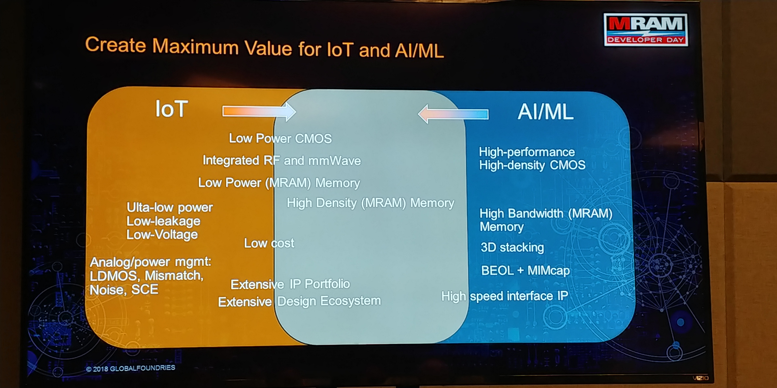
12:58PM EDT - AI/ML all about the datacenter - high performance, high speed IP etc
12:58PM EDT - IoT is all about the small chips and ultra low leakage
12:58PM EDT - Only high-density MRAM can really connect the two

12:59PM EDT - 22FDX is low power fully depleted SOI process
01:00PM EDT - Can run A53 at almost 2 GHz
01:00PM EDT - Lower dynamic and leakage
01:00PM EDT - 22FDX is king of power
01:00PM EDT - Uses back-biasing to help boost perf, or reduce back-bias to lower VTs and still run fast
01:01PM EDT - Overall 80% lower power
01:01PM EDT - Best in class mmWave perf
01:01PM EDT - eMRAM for NVM
01:01PM EDT - Increasing value prop by coupling eMRAM

01:02PM EDT - Ecosystem is already quite large, and growing
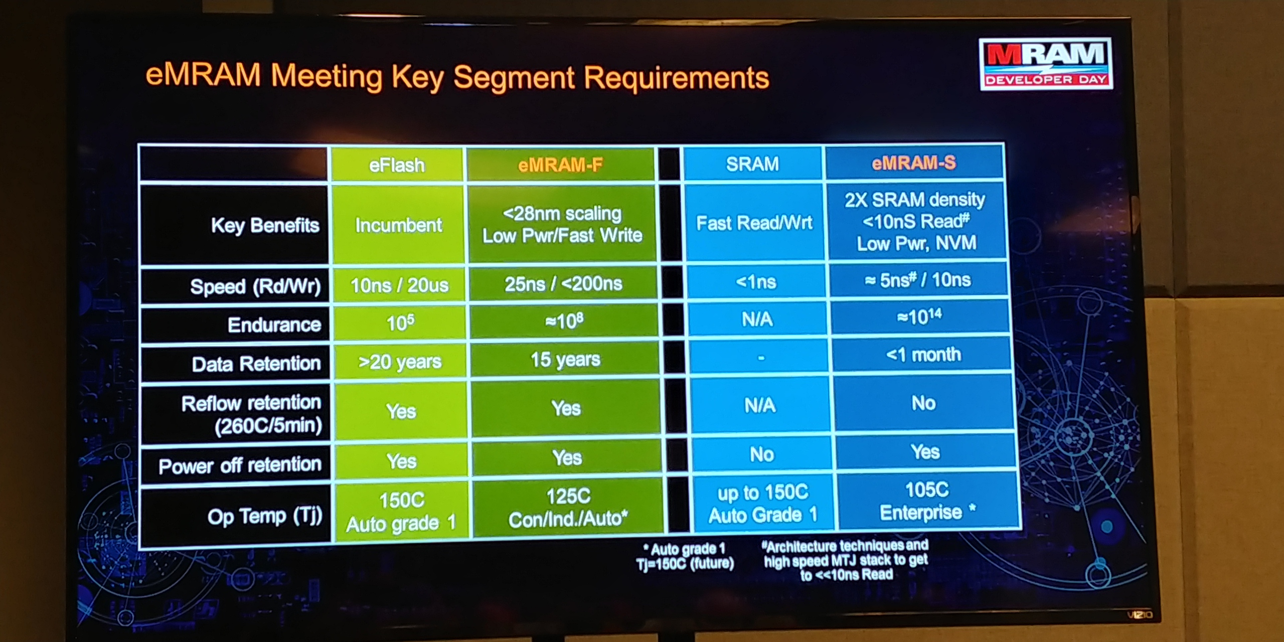
01:03PM EDT - Two versions of MRAM: -F for flash replacement, -S for SRAM replacement
01:04PM EDT - Differences in speed, endurance, data retention, operating temperature
01:05PM EDT - eMRAM-F is a cold storage technology, hence 15 year data retention
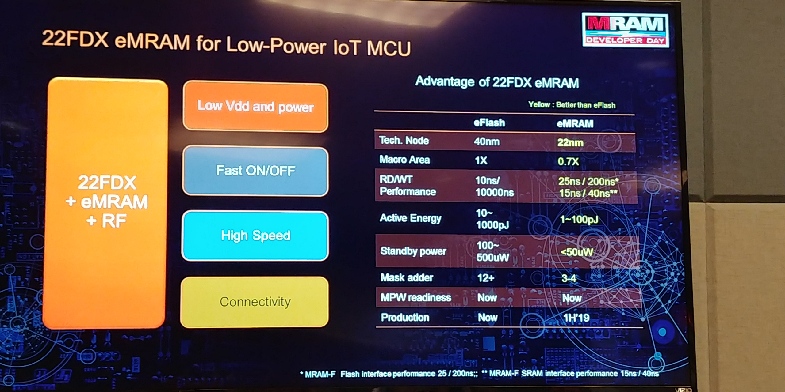
01:05PM EDT - eMRAM on 22FDX beats eFlash on 40nm
01:06PM EDT - Production of 22FDX eMRAM set for 1H 2019
01:07PM EDT - Status of 22FDX eMRAM
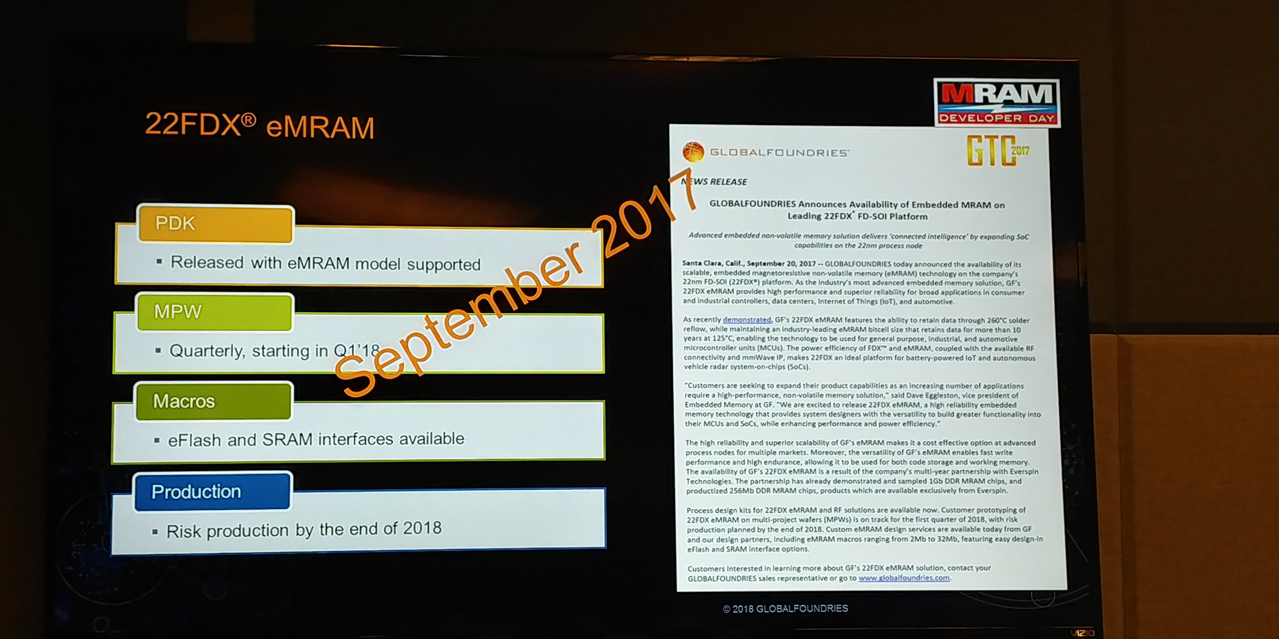
01:07PM EDT - Quarterly MPWs starting in Q1 2018
01:07PM EDT - Risk production by end of 2018
01:07PM EDT - JDV with Everspin in 2014
01:08PM EDT - Succeeded in each area
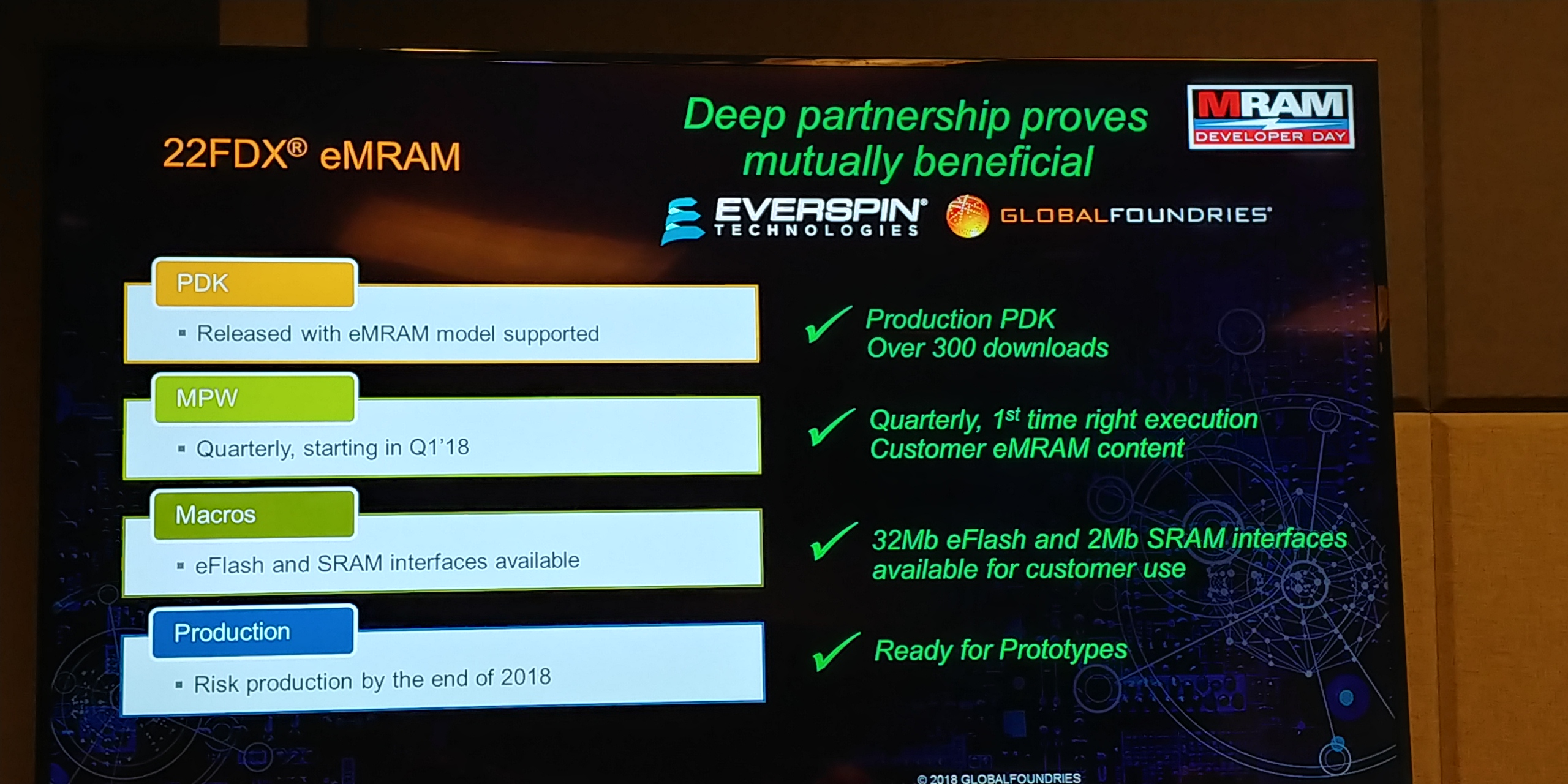
01:08PM EDT - 300 companies using production PDK
01:08PM EDT - 32Mb eFlash and 2Mb SRAM interfaces available for use
01:10PM EDT - Already announced $2b of design wins on 22FDX, most of which with eMRAM involved

01:10PM EDT - Next gen is 12FDX
01:10PM EDT - 7nm FinFET power efficiency with body bias, but still FDSOI planar process
01:11PM EDT - 40% fewer masks than 7nm DUV
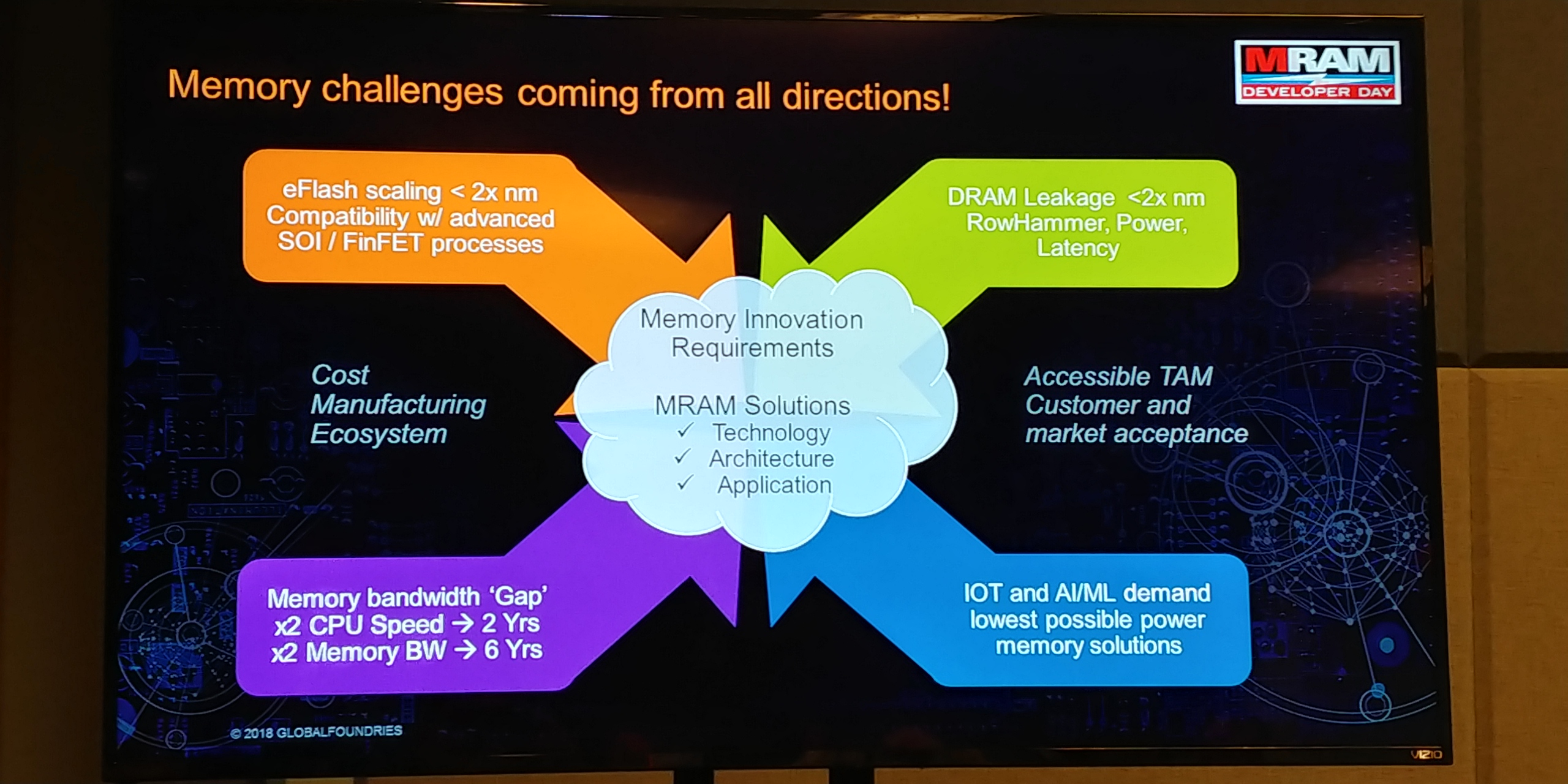
01:12PM EDT - Four arms of technical challenges
01:12PM EDT - Never underestimate incumbents: eFlash scaling for example
01:13PM EDT - DRAM below 22nm is still in development - data integrity and corruption is a concern
01:13PM EDT - eDRAM has run out of steam
01:13PM EDT - SRAM Memory bandwidth is lagging behind CPU perf
01:13PM EDT - MRAM could help catch up
01:14PM EDT - IoT demand for lowest possible power memory solutions
01:14PM EDT - Non-technical challenges - cost of manufacturing ecoysystem, market acceptance
01:15PM EDT - making all the TAM accessible
01:15PM EDT - A lot of people want to go with the proven solution - hard to drive adoption without a compelling product
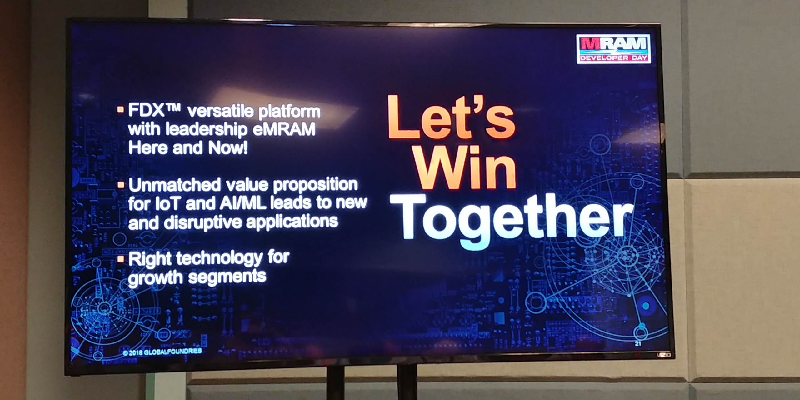
01:16PM EDT - MRAM is ready for GF customers


1 Comments
View All Comments
abufrejoval - Monday, August 6, 2018 - link
So if I understand correctly, you can have MRAM on your SoC today,1. if you port your IP blocks to their 22nm process (but they have an A53 ready to use)
2. you can choose between a high-density, long retention but slower variant to do 'storage things' and a lower-density, shorter retention variant to replace SRAM and DRAM tiers, if you can live with 5-10x slower access times vs. SRAM, but 2x areal density to 6T SRAM
3. Costs you 4 extra layers, gains you non-volatility for the MRAM
Sounds like an interesting niche.