Covert Ops in Taiwan - Intel Tejas & Socket 775 Unveiled
by Anand Lal Shimpi on January 9, 2004 10:49 AM EST- Posted in
- CPUs
While the majority of the AnandTech staff was hard at work in Las Vegas covering CES, a quiet staff member was touring the streets of Taipei.
During his visit to Taipei he came across some information shared by some very good contacts about Intel's Prescott successor - Tejas. Very few people caught on to the fact that we actually talked about Tejas on AnandTech years ago as we heard about the codename before Prescott and even before Northwood, hidden in an Intel presentation that hadn't properly been cleaned up. Originally Tejas was listed as the first Intel CPU to have a 1.2GHz FSB, but now we know a bit more about the CPU.
Apparently a total of 10 Tejas samples have been shipped out to various friends of Intel, all running at 2.8GHz. What's also interesting to note is that our sources have informed us that at 2.8GHz Tejas uses around 150W of power - about 50% more than Prescott at the same clock speed.
Given that Tejas is still a 90nm part, it would be unlikely that the additional power consumption would be due to a larger cache as that would make the die huge and isn't Intel's style to increase cache size without shrinking the die further. If the power figures we've been given are indeed correct, one possible explanation would be that Tejas is indeed some variation of a multicore CPU. While it is unlikely that Tejas includes two discrete Prescott cores on die, there is a chance that the two cores (if they exist) could be sharing data caches and maybe other units. A multicore Tejas would explain the jump in power consumption, and it is in line with Intel's strategy although it does seem sooner than expected.
The 10 Tejas samples are all LGA-775 CPUs and luckily our contact was able to gather some pictures of the CPU and the interface so you all can get a glimpse of what is soon to come. We had to blur out some parts of the pictures to protect the identity of our sources, but you'll still be able to see what's important.
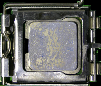
In the shot above you'll see the Tejas as it appears immediately after you remove the heatsink. There is a lever at the top of the picture that you can barely see that will allow you to remove the CPU. Unlatching the lever will result in the picture below. The metal covering can now be pulled up thus exposing the CPU, which can easily be removed:
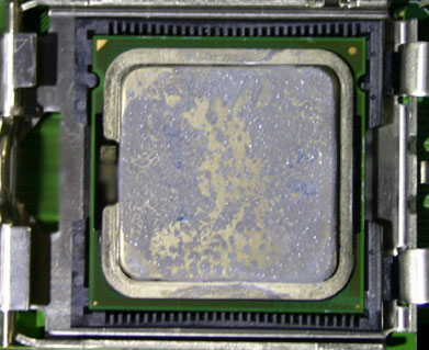
The notches on either side of the CPU at the top of the picture prevent it from being inserted improperly and also help line up the contact points on the bottom of the CPU.
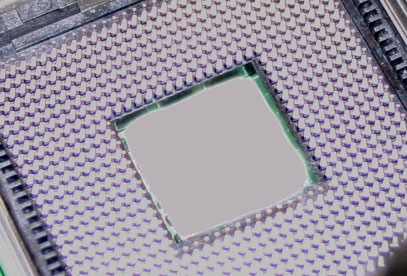
Before we look at the bottom of the CPU itself, let's look at what's underneath the CPU - a bed of pins (note that we purposefully blocked out some of what was in the middle of the pins):
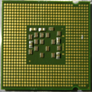
Now to flip the chip over we've got a nice look at the flat surface of the pinless CPU - welcome to LGA-775. This is the same CPU interface that you'll find on Prescott CPUs after April, but what you're looking at here is Tejas as far as we know.
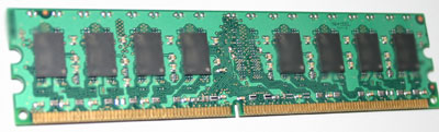
As an added kick here's a DDR-II module out of the Tejas system:
There you have it; no benchmarks, not a lot of information, but some interesting pictures and hopefully something to think about for what happens after Prescott...


27 Comments
View All Comments
cyberphant0m - Monday, February 23, 2004 - link
looks like the DDR2 module has around 230+ pins. Truly a revolutionary step in memory IMHOmechBgon - Sunday, January 11, 2004 - link
Figure the motherboard's voltage circuitry to be about 75% efficient and that translates to ~200W draw at the motherboard. I wonder if this will cut down on the scoffing I sometimes hear when I recommend a 400W+ power supply... : )INTC - Sunday, January 11, 2004 - link
And once again CRAMITPAL talking trash about stuff that he knows nothing about. Right on the Ace's Hardware homepage is an article on Prescott that says:"...here are some (absolute) maximum power values:
0.09 µ Pentium 4 "Prescott" 3.4 GHz: 86-93W"
AMD's own thermal data sheet for Athlon 64/FX says 89W max http://www.amd.com/us-en/assets/content_type/white...
Commenting on an unreleased processor is funny coming from CRAMITPAL - the true "FLAMEthrower" in this forum.
CRAMITPAL - Sunday, January 11, 2004 - link
Actually this subject has been discussed in considerable detail and the current 3.2 Gig. Piss 4/Prescott both use almost DOUBLE the electrical power of an equal speed rated A64 CPU. Ace's Hardware has the typical thermal dissipation figures and they are 50-60W for A64 and 100+ W for Piss 4/Prescott at 3.2 Gigs. When you calculate the additional power needed for the additional case fan(s) and larger/faster CPU fan for the Prescott, and the air-conditioning bill, the TCO for enterprise is staggering to use Prescott compared to the A64, and Prescott don't even do 64 bit apps.A typical U.S. University spends a MILLION dollars per month on electricity. Conservative cost analysis has shown that with A64 systems instead of P4/Prescott systems, a university could save 10% or more per month forever compared to the P4/Prescott. For those who can't do the math, that's a HUNDRED GRAND per month, every month. While the utility companies may love Prescott, you won't be seeing them in enterprise any time soon. The Mobo mfgs. are VERY unhappy with Intel as Prescott is gonna kill enterprise sales. Thankfully for most (but not all) Mobo makers, Opteron/A64 will fill the void created by Prescott.
And despite the daydreaming Tejas ain't a dual-core chippie, yet at 2.8 Gigs. it does use close to 150W due to large caches. Smart investor should be buying stock in water cooling, fire extinguishers, insurance companies, and fire suits if ya wanna profit from Intel's Flame Throwers.
The Times, they are a changin'
Idoxash - Saturday, January 10, 2004 - link
... I dun know about you guys but besides the heat have you thot about the energy bill? This things eats up 150 watts by it self and that's not countting the rest of the system. You ask me I know VIA does not have the most powerful of cpus but they heading a far better diretion with their cheap/super cool cpus. I guess you can always say GAMES it's all about the GAMES! I think I go back to console and mobile gaming.--Idoxash
Cygni - Saturday, January 10, 2004 - link
On second thought, i might be thinking of some other codename that started with T...Cygni - Saturday, January 10, 2004 - link
I think Tejas was originally the code name for an Intel "all in one" chip that integrated literally everything into one major die, some 2-3 years ago. He mentions it a little... I think they even got to sampling before killing the project.I too am sick of the rapid socket changes. Intel isnt the only guilty party... way too many AMD sockets as well.
And that is a CRAZY mounting system...
sprockkets - Saturday, January 10, 2004 - link
Why wouldn't SOI work? Intel's future manu process will do SOI but with further treaking of the process.Haven't we already seen the new core of Prescott? Perhaps we saw the P4 at 90, but not prescott? It's smaller than what we have now. Chip architech had something on that.
If you ask me why not commment on the fact that Anand's review had the 2.8 ghz Intel processor hidden from view? He of all people should know when it comes out.
So much for making loads of money off of Prescott in q4 Intel.
Dug - Friday, January 9, 2004 - link
"We had to blur out some parts of the pictures to protect the identity of our sources"Shouldn't be too hard to figure out if there's only 10 samples out there :)
mkruer - Friday, January 9, 2004 - link
Just to poke fun at some of the other sites namely toms hardware.But if it is true that AMD are running hot and that the Athlon64 line runs at 85watts Then there is no way in hell (pun intended) that the tejis will ever run cooler then 140watts., because apparently according to them SOI doesn’t work.