Kopin at CES 2017: 2K120 VR, Whisper Voice Recognition
by Joshua Ho on January 6, 2017 7:00 AM EST- Posted in
- Mobile
- Displays
- AMOLED
- Trade Shows
- Voice Processors
- VR
- OLED
- Kopin
If you’ve never heard of Kopin before, you’re probably like most people. Going into CES I had no idea what Kopin was, but it turns out that they’re actually a fairly significant company that has been around for decades working on microdisplay technology after spinning off from MIT’s Lincoln Labs. Naturally, as a spin-off of a DoD lab their primary revenue currently comes from the US government/DARPA, which is willing to fund rather expensive projects like microdisplay technology as it has applications in systems like the F-35 JSF, which has a Kopin microdisplay in the helmet along with microdisplays for systems like thermal weapon sights, night vision goggles, laser rangefinder/designators, TOW launcher sights, and advanced rifle sights like the Trijicon CCAS.
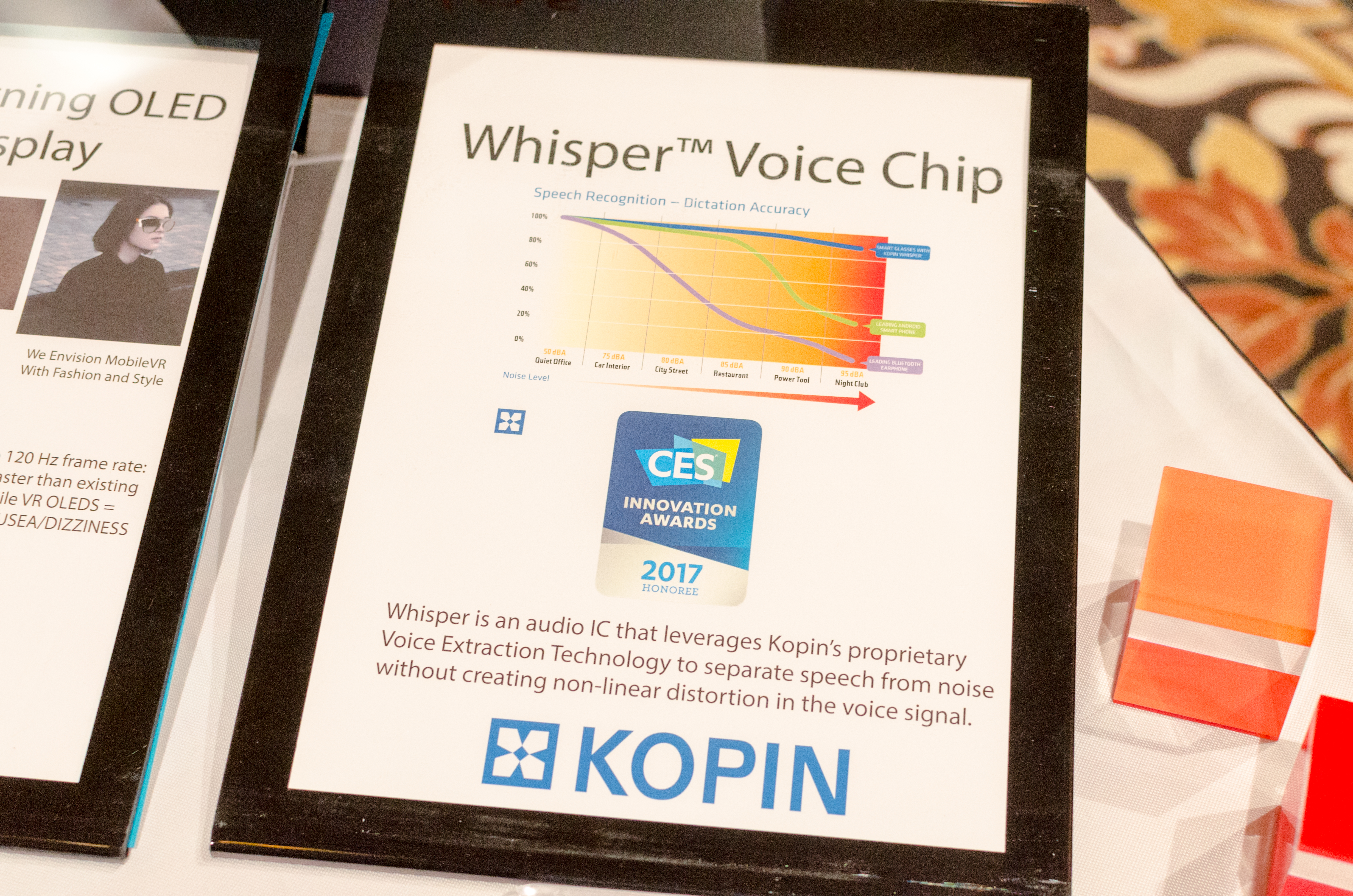
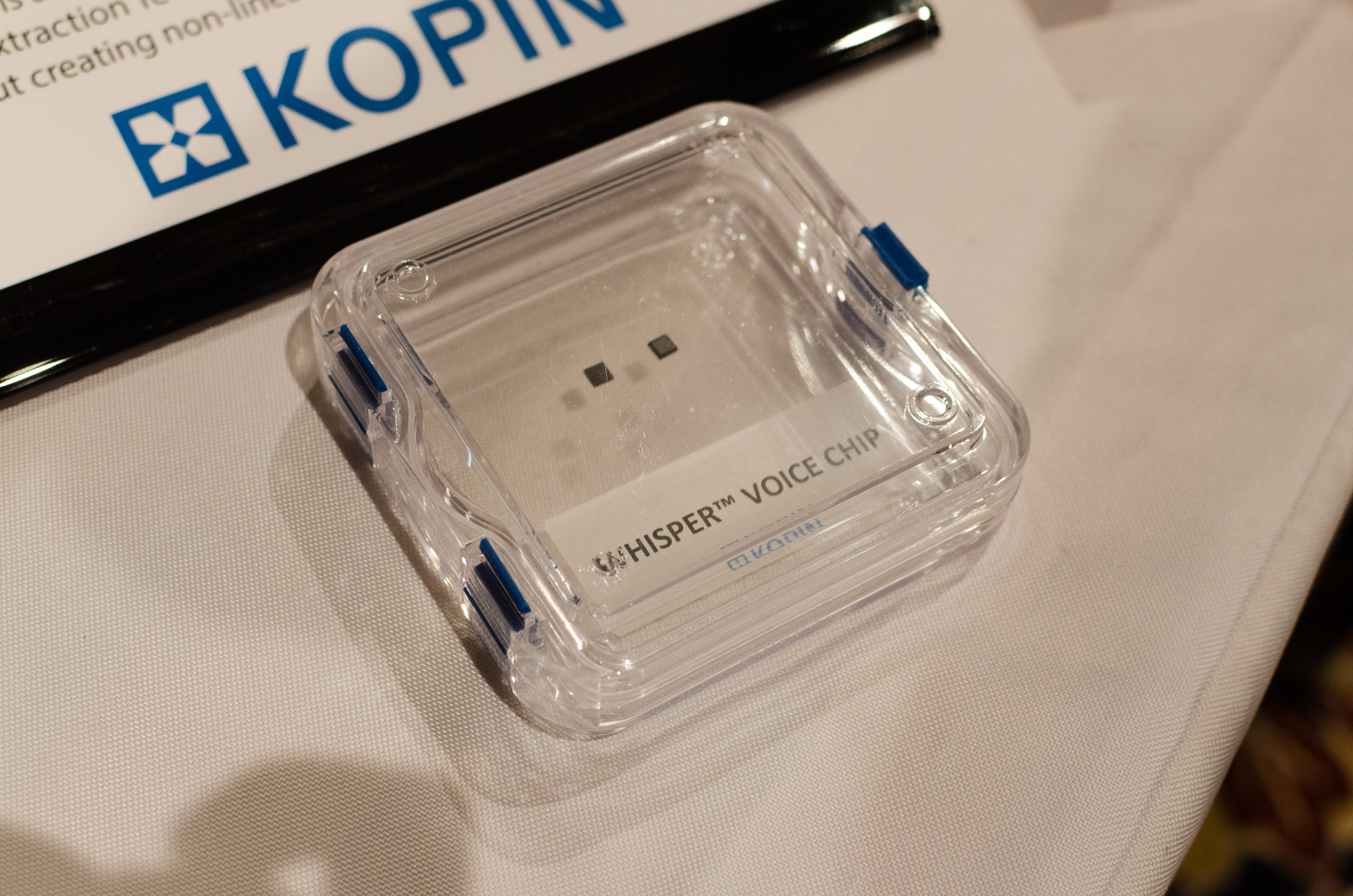
For CES, Kopin had a number of interesting new products to show off, chief among which was the Whisper voice chip. They were relatively cagey about discussing the specifics of implementation here but the essence is that rather than attempting to subtract out noise, Kopin’s approach attempts to extract out the voice signal to improve reliability for voice command applications. They claim this dramatically improves accuracy in high-noise environments relative to existing solutions commonly seen in smartphones, but I wasn’t able to necessarily prove this when playing around with a babble track and the demo equipment which was around 80 dBA. Power is said to be less than 10 mW and output uses the common i2s interface.
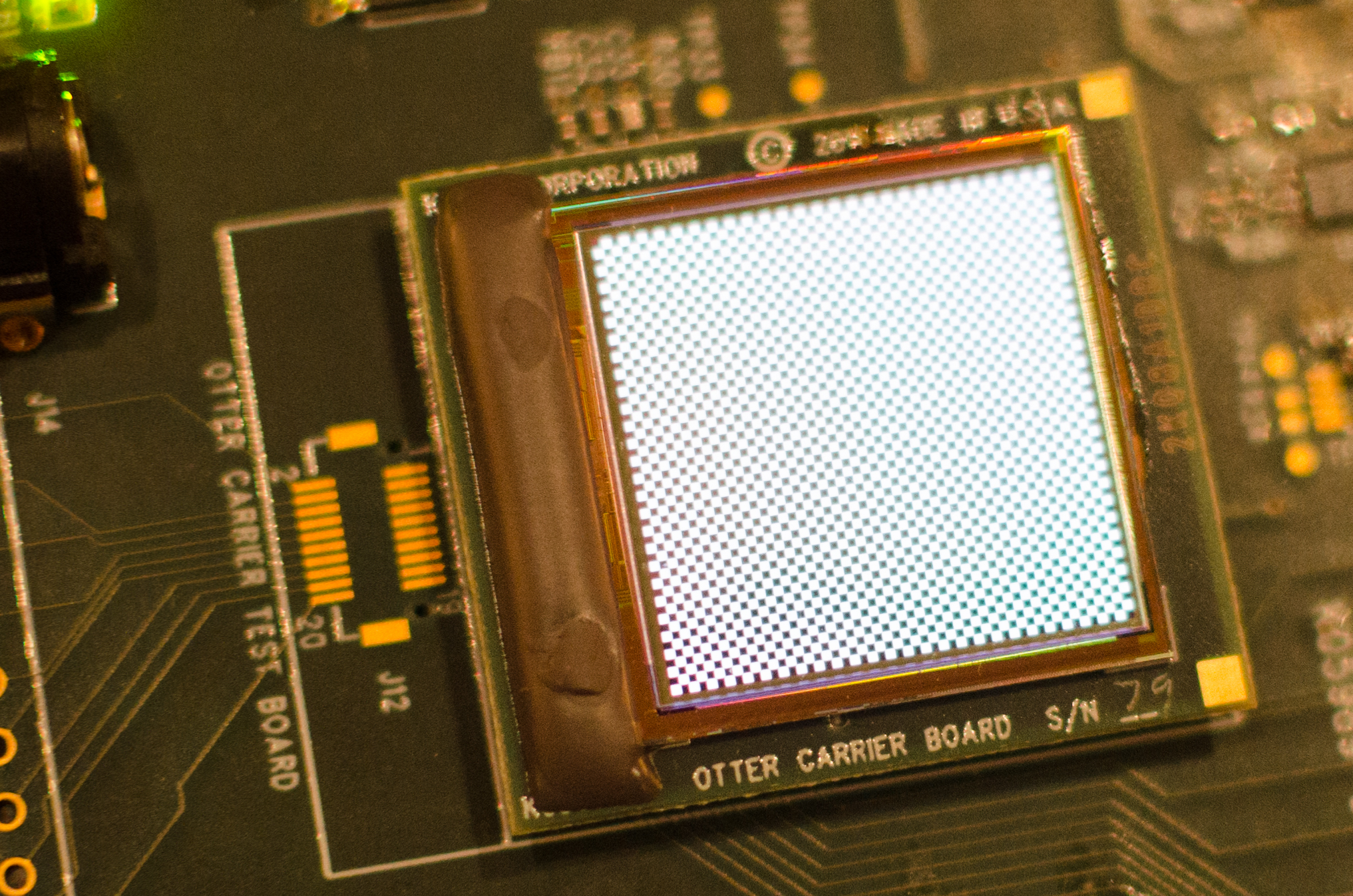
Probably the most interesting product shown was their OLED “Lightning” microdisplay designed for VR. With a 2048x2048 resolution and a 1 inch diagonal size it has 2925 pixels per inch and actually achieves this properly with red, green, and blue subpixels per pixel rather than two subpixel arrangements like PenTile. While they weren’t going to divulge the exact details on how this is achieved, in essence by creating the TFT backplane from a single crystal of silicon and slicing the substrate such that the wafer is only about 100 angstroms thick, the backplane is translucent and can be used to create the active matrix for LCDs and OLED displays.
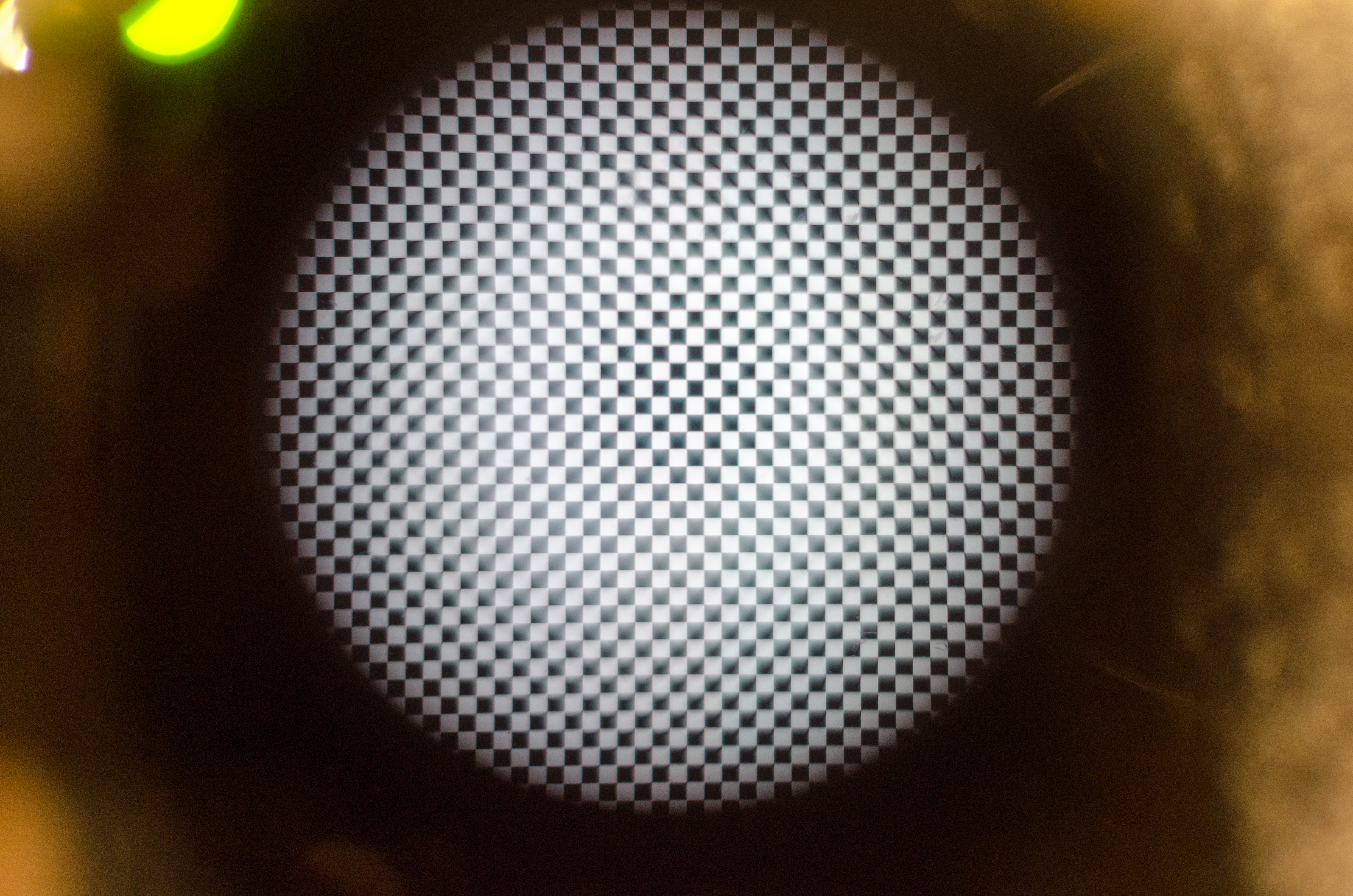
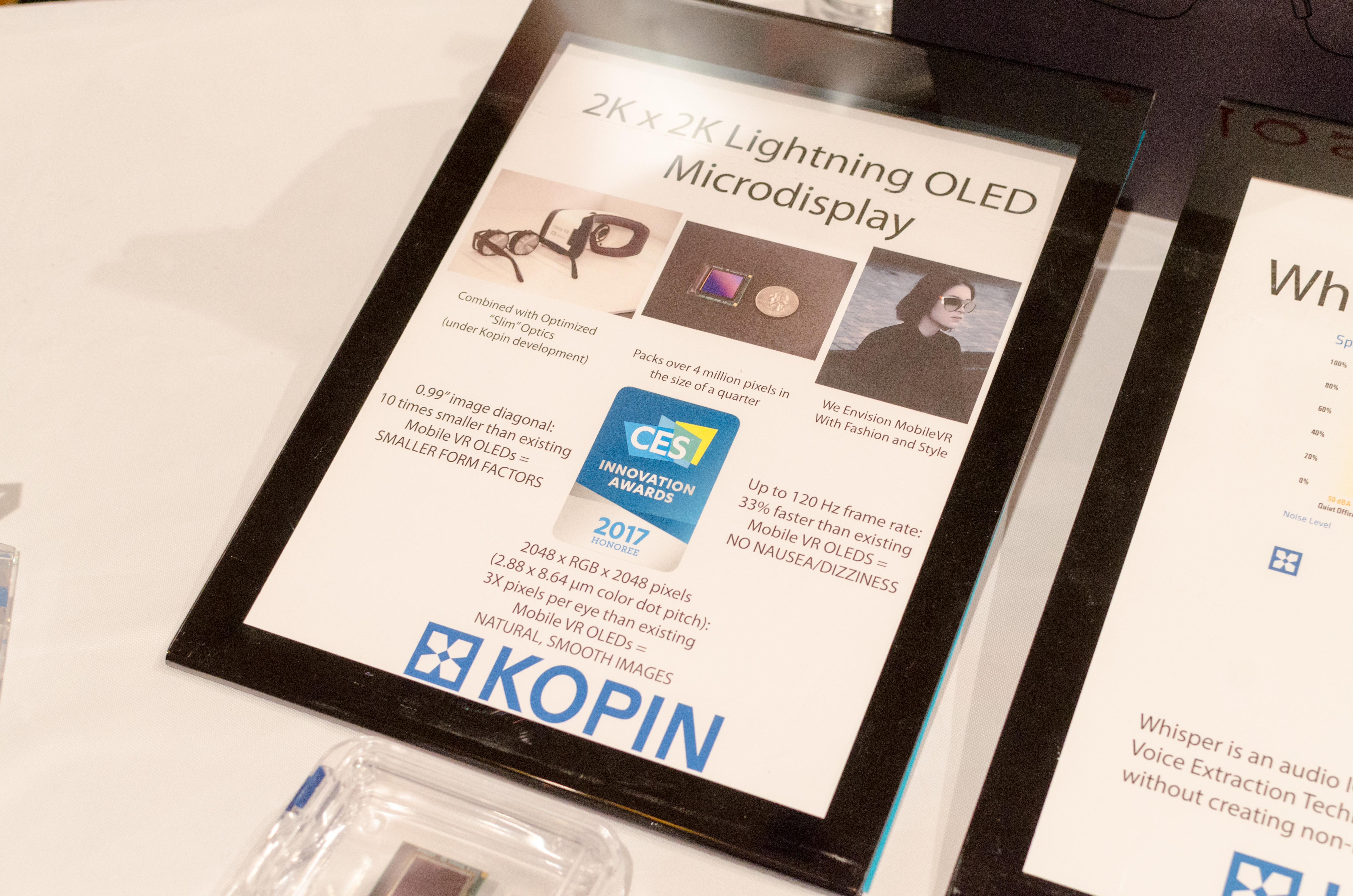
This method also allows for common circuitry like the display driver to be integrated into the backplane which dramatically reduces bezel requirements. Of course, the cost of such methods is non-trivial so we won’t be seeing such methods in smartphones any time soon, but such displays can work for VR with the right optics. If you study the principles behind the design of semiconductor devices you’ll know that using polysilicon and/or amorphous silicon are going to adversely impact device properties due to defect states that impact things like recombination lifetime and carrier mobility. By using this single crystal silicon method, in addition to a high 2048x2048 resolution, the display refreshes at 120Hz with 10 microsecond latency and has a high fill factor above that commonly seen in smartphone AMOLED displays along with low power consumption.
Seeing is believing here, and I quite literally could not see anything resembling aliasing on the display even with a 10x loupe to try and look more closely at the display. The ultimate test here would be Vernier acuity, but due to the early state of the device it was simply running a demo loop of test patterns rather than any arbitrary displayed image. Using slow motion 240 FPS capture I was unable to see any flickering or similar issues.

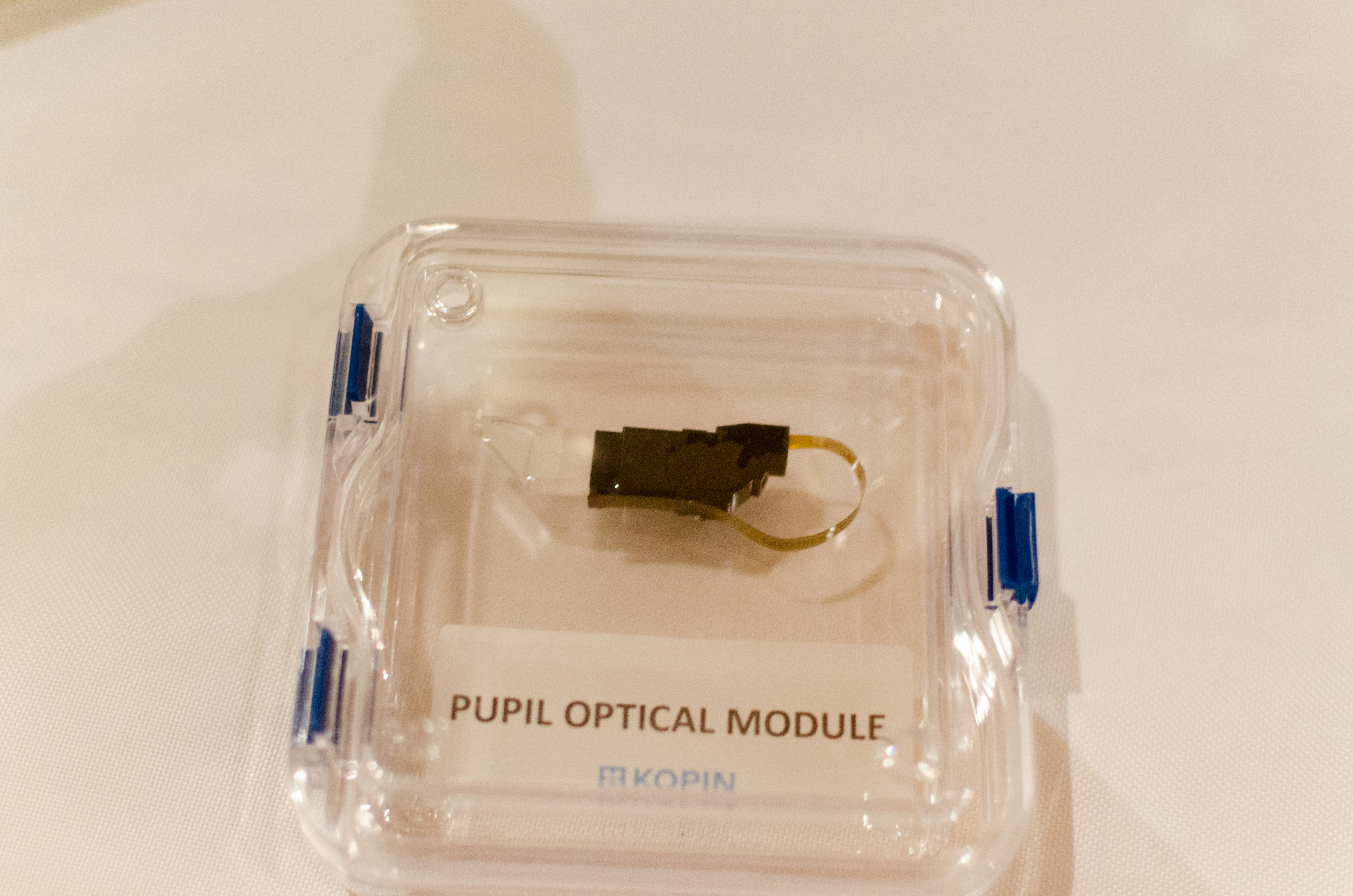
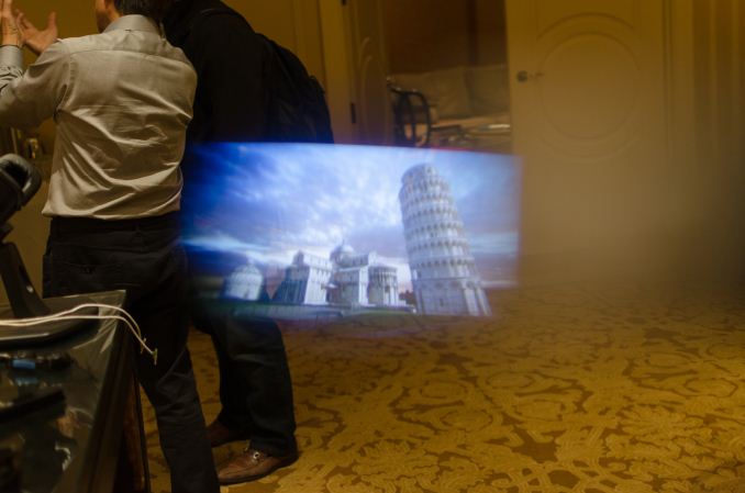
In addition to these announcements, Kopin also launched a new Pupil optical module which is said to be the smallest optical LCD module for smart glasses which seems to work fairly well when I tried it out. Resolution is nHD, or 640x360 but considering the size it’s within expectations. Overall, I try to find something truly interesting and innovative at CES every year and I think Kopin is one of the few companies really doing something that I haven’t seen before.


5 Comments
View All Comments
nathanddrews - Friday, January 6, 2017 - link
"2048x2048 resolution, the display refreshes at 120Hz with 10 microsecond latency"Finally a replacement for CRT!
p1esk - Friday, January 6, 2017 - link
"slicing the substrate such that the wafer is only about 100 angstroms thick"100 angstroms is 10nm. There's no way to slice anything this thin. The thinnest wafer I've heard of is about a micron thick.
JoshHo - Sunday, January 8, 2017 - link
I suspect the true process is a trade secret and one that is closely protected as such technologies have national security value.MrSpadge - Tuesday, January 10, 2017 - link
It could be a 10 nm Si layer on a SOI wafer, where they remove the carrier wafer and have 2 - 3 µm of SiO2 as "buffer" for the thinning.LordanSS - Saturday, January 7, 2017 - link
Welps, this kind of display technology is several years away from regular consumer technology. But when the time comes, it sure would be quite nice.Who knows, maybe on the third generation of (current) VR headsets this thing might be around, or at least something with half the ppi (which would be quite good already).