Intel Launches 7th Generation Kaby Lake: 15W/28W with Iris, 35-91W Desktop and Mobile Xeon
by Ian Cutress on January 3, 2017 12:01 PM ESTA New Optimized 14nm Process: 14nm+
As originally reported in the Kaby Lake-Y/U Launch
One of the mysteries with the launch of Kaby Lake is the optimized 14nm+ process that Intel is promoting as one of the key components for the performance uptick in Kaby Lake. It’s worth noting that Intel has said nothing about caches, latencies or bandwidths. We are being told that the underlying microarchitecture for Kaby Lake is the same as Skylake, and that the frequency adjustments from the new process, along with features such as Speed Shift v2 and the new fixed function media codecs, account for the performance improvements as well as battery life increases when dealing with 4K content.
For users that speak in pure IPC, this may/may not be a shock. Without further detail, Intel is implying that Kaby Lake will have the same IPC as Skylake (which we can confirm in our reviews), however it will operate with a better power efficiency (same frequency at lower power, or higher frequency at same power) and for media consumption there will be more idle CPU cycles with lower power drain. The latter makes sense for mobile devices such as tablets, 2-in-1s and notebooks, or for power conscious users, but paints a static picture for the future of the desktop platform in January if the user only gets another 200-400 MHz in base frequencies.
However I digress with conjecture – the story not being told is on how has Intel changed its 14nm+ platform. We’ve only been given two pieces of information: taller fins and a wider gate pitch.

Intel 14nm Circa Broadwell
When Intel launched Broadwell on 14nm, we were given an expose into Intel’s latest and greatest semiconductor manufacturing lithography node. Intel at its core is a manufacturing company rather than a processor company, and by developing a mature and robust process node allows them to gain performance advantages over the other big players: TSMC, Samsung and GlobalFoundries. When 14nm was launched, we had details on their next generation of FinFET technology, discussions about the issues that faced 14nm as it was being developed, and fundamental dimensional data on how transistors/gates were proportioned. Something at the back of my brain says we’ll get something similar for 10nm when we are closer to launch.
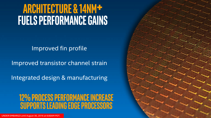
But as expected, 14nm+ was given little extra detail. What would interest me is the scale of results or the problems faced by the two changes in the process we know about. Taller fins means less driving current is needed and leakage becomes less of an issue, however a wider gate pitch is typically associated with a decrease in transistor density, requiring higher voltages but making the manufacturing process easier with fewer defects. There is also the argument that a wider pitch allows the heat generation of each transistor to spread more before affecting others, allowing a bit more wiggle room for frequency – this is at least how Intel puts it.
The combination of the two allows for more voltage range and higher frequencies, although it may come at the expense of die size. We are told that transistor density has not changed, but unless there was a lot of spare unused silicon in the Skylake die design for the wider pitch to spread, it seems questionable. It also depends which part of the metal stack is being adjusted as well. It’s worth noting that Intel has not released die size information again, and transistor counts as a metric is not being disclosed, similar to Skylake.
Finally, there's some question over what it takes at a fab level to produce 14nm+. Though certainly not on the scale of making the jump to 14nm to begin with, Intel has been tight-lipped on whether any retooling is required. At a minimum, as this is a new process (in terms of design specifications), I think it's reasonable to expect that some minor retooling is required to move a line over to 14nm+. In which case the question is raised over which Intel fabs can currently produce chips on the new process. One of the D1 fabs in Oregon is virtually guaranteed; whether Arizona or Ireland is also among these is not.

I bring this up because of the parallels between the Broadwell and Kaby Lake launches. Both are bottom-up launches, starting with the low wattage processors followed by the bigger parts a few months later. In Broadwell's case, 14nm yields - and consequently total volume - were a bottleneck to start with. Depending on the amount of retooling required and which fabs have been upgraded, I'm wondering whether the bottom-up launch of Kaby Lake is for similar reasons. Intel's yields should be great even with a retooling, but if it's just a D1 fab producing 14nm+, then it could be that Intel is volume constrained at launch and wanted to focus on producing a larger number of small die 2+2 processors to start with, ramping up for larger dies like 4+2 and 4+4e later on.


43 Comments
View All Comments
hans_ober - Tuesday, January 3, 2017 - link
i7-7820HK typo: boost frequency of 4.9GHzkenansadhu - Tuesday, January 3, 2017 - link
Oh it was a typo? I was so happy to see that. So what's the correct boost speed? I'm also curious about the price. Is it actually not more expensive than other i7 models?midspace - Tuesday, January 3, 2017 - link
should be Boost of 3.9Ghzhttp://ark.intel.com/products/97464/Intel-Core-i7-...
hansmuff - Tuesday, January 3, 2017 - link
Fist time I read about the AVX Offset feature.. pretty cool and I'm looking forward to benchmarks playing with it. I wonder what AMDs chips will do with regards to that, I can only assume they have similar thermal issues with those instruction sets.ddriver - Tuesday, January 3, 2017 - link
TICK TOCK MEHMr Perfect - Tuesday, January 3, 2017 - link
"Calculating Generational IPC Changes from Sandy Bridge to Kaby Lake"Looking forward to this one, as I've still got an i7-2600 kicking it in my machine. Maybe we can declare Sandy Bridge dead again? ;)
kmmatney - Tuesday, January 3, 2017 - link
The performance improvement from Skylake is minimal. If Skylake wasn't enough to upgrade, then Kaby lake won't be either. If you have a 2600K, especially overclocked, then you are better off buying other improvements - such as SSDs or better video cards, which you can still take along whenever you do upgrade.My personal upgrade strategy over the last 20 years was to upgrade whenever I could double my performance at the same price. I can still do this with video cards, but not with cpus.
Cellar Door - Tuesday, January 3, 2017 - link
You completely missed the sarcasm in Mr Perfect's post.And as far as upgrade strategies go, it basically always comes down to what your wallet can handle and its not black and while 2x perf. increase.
EX. new VP9 hw decode - perfect for laptops, yet nowhere near 2x perf increase in all other areas.
esterhasz - Tuesday, January 3, 2017 - link
I think that kmmatney had desktops in mind...But yeah, I'm actually pretty excited for KL in laptops. YouTube is pushing VP9 really hard and I'm curious what the Iris+ 650 will be able to do. No miracles for sure, but coming from a Haswell U-Series chip, the time's finally ripe for an upgrade.
Mr Perfect - Tuesday, January 3, 2017 - link
Yeah, that exactly what I've been doing. A 1TB 850 Evo, Windows 10 and a GTX1060 made the 2600 completely relevant again. I'm actually still feeling the limit of the GPU, volumetric lighting in Fallout 4 is too much for the 1060.