Toshiba Finalizes Plans for New 3D NAND Fab: Coming Online in 2019
by Anton Shilov on November 15, 2016 9:30 AM EST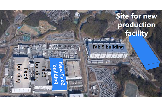
Toshiba in the past week has finalized plans to build a new production facility to make 3D NAND flash memory. The company will start construction in early 2017 and in addition to a new manufacturing site Toshiba will also build a new R&D center. Toshiba is still talking with its partner Western Digital about joint investments in the new facility, but no matter what, the building will be completed in mid-2018 and the fab will start high volume production in 2019.
Toshiba intends to start construction of the first phase of its new fab in February 2017 and no decisions about the second phase of the project have been made so far. The building is set to be complete inside and out sometime in summer 2018 and then the company will have to move in equipment, which takes two to three quarters. If everything goes smoothly, the fab will produce its first 3D NAND wafers in late 2018, but high volume commercial production will start in calendar 2019. We are told that the building will have a quake-absorbing structure and will also use an environmentally friendly design that includes LED lighting.
The manufacturer will finalize decisions regarding exact production capacity as well as equipment investment sometime next fiscal year, which begins in April 2017 for Toshiba. While the company does not indicate planned capacities, it disclosed plans to use an AI-powered production system to boost productivity. Toshiba says that its decisions will reflect market trends, but given the fact that NAND flash memory is in short supply today, it is could be expected that the company to max out the capacity in the first phase of its next fab. Another reason why Toshiba might want to maximize production capacity of the manufacturing facility is due to the aggressive expansion of production capacities by Samsung. At the moment, Toshiba and Western Digital (which acquired Toshiba’s partner SanDisk) produce more NAND flash at the Yokkaichi Operations memory production complex in Mie prefecture than any other manufacturer and Toshiba would certainly like to keep it that way.
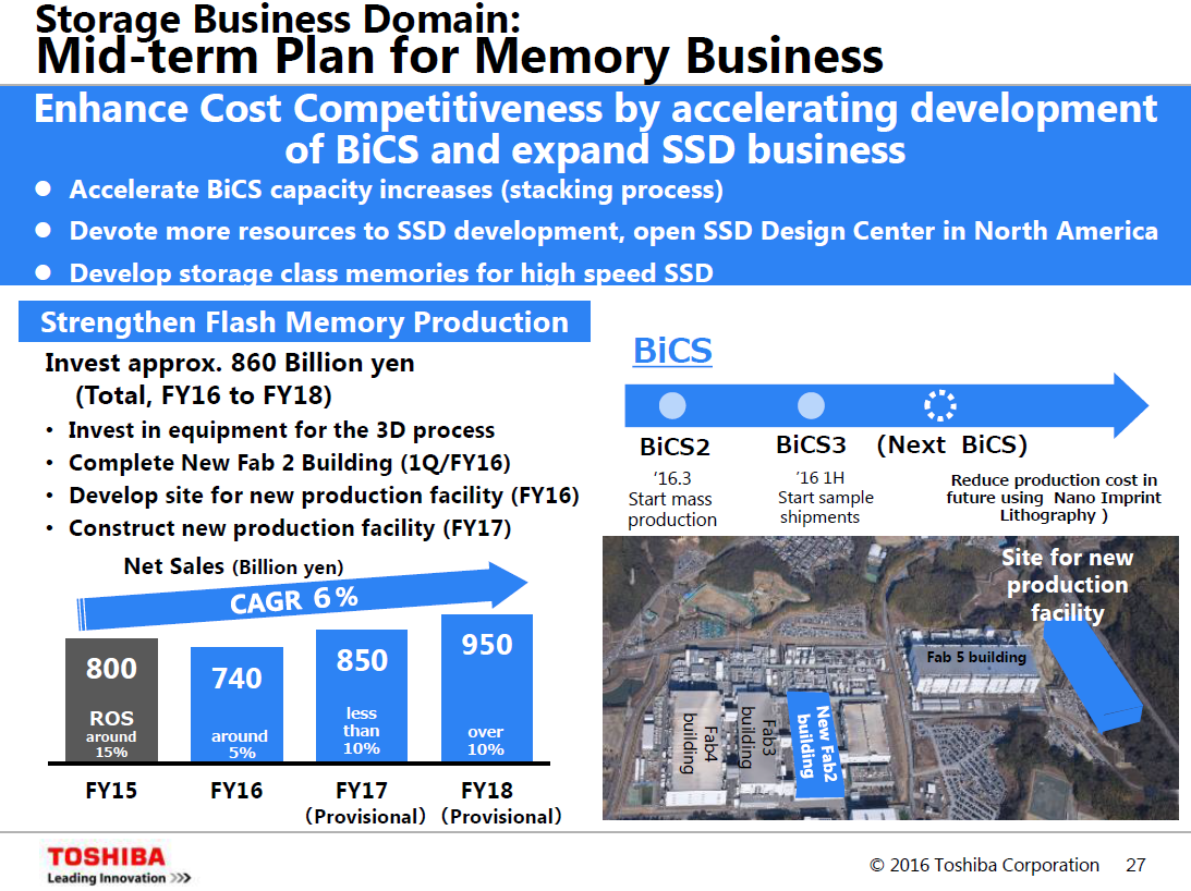
In addition to the new production facility, Toshiba also plans to build a new memory research and development center adjacent to the fab. The NAND flash maker intends to bring together R&D activities now carried out at different sites to the new center in a bid to speed up development. Moreover, bringing R&D and production close to each other simplifies certain processes and that could result in better competitive positions of the company over time.
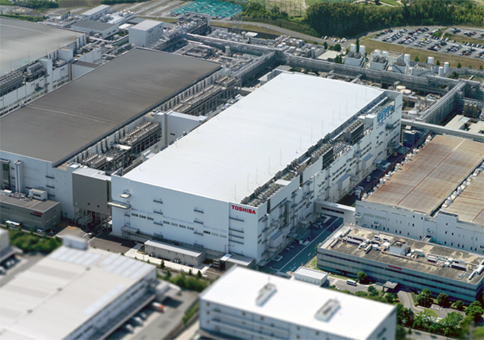
As outlined multiple times, Toshiba’s new fab will exclusively make the company’s proprietary 3D NAND memory, which the company calls BiCS (Bit Cost Scalable) NAND. Toshiba claims that due to its U-shaped NAND string, BiCS is more efficient in terms of die sizes compared to other types of 3D NAND (this is something that has yet to be confirmed by independent researchers). Today, Toshiba and Western Digital produce 3D NAND flash in their recently opened Fab 2 (pictured below). Also, the two companies have begun to convert the Fab 5 to 3D NAND. Therefore, three years from now, Toshiba and Western Digital (assuming that the latter invests in the new fab) will have three manufacturing facilities producing 3D NAND. However, before that happens, the companies will have to rely on architectural improvements (of 3D NAND), conversion of the Fab 5 and minor improvements of actual capacities in existing fabs as primary means to rise bit and chip output. It remains to be seen how significantly the companies manage to increase their output in the coming years and whether the short supply of NAND flash is set to persist.
Right now Toshiba and Western Digital produce 48-layer BiCS 3D NAND memory commercially. This type of flash is used for embedded and removable applications, but not currently for SSDs (except Toshiba’s BGA SSD introduced earlier this year). Western Digital recently confirmed that its clients had received samples of 64-layer BiCS NAND chips and the company was on track to start volume production of such ICs in the first half of calendar 2017. Perhaps, 64-layer BiCS NAND by Toshiba/Western Digital will finally be used inside SSDs.
Source: Toshiba


8 Comments
View All Comments
JoeyJoJo123 - Tuesday, November 15, 2016 - link
Too little too late. By then, Samsung will have that much bigger of a lead over everyone else... :\fanofanand - Tuesday, November 15, 2016 - link
Maybe so, but hopefully not. Wintel has shown us what kind of products the consumer gets when there is little to no competition.prisonerX - Tuesday, November 15, 2016 - link
So has Apple.DanNeely - Tuesday, November 15, 2016 - link
What are Fabs 3 and 4 (and 1???) producing? If NAND is Toshiba expecting there to still be a large market for planar NAND several years from now, or are they making something different in those buildings?extide - Thursday, December 8, 2016 - link
Probably planar NAND. I bet they will all be converted eventually.evancox10 - Tuesday, November 15, 2016 - link
But where is it? City/country?Billy Tallis - Tuesday, November 15, 2016 - link
Yokkaichi, Mie Prefecture, Japan.SetiroN - Tuesday, November 15, 2016 - link
That's some professional drawing right there.