Original Link: https://www.anandtech.com/show/2869/p55-overclocking-showdown-asus-gigabyte-and-evga-at-the-oc-corral-page-6-updated-
P55 Overclocking Showdown - ASUS, Gigabyte, and EVGA at the OC Corral (Page 6 Updated)
by Rajinder Gill on November 6, 2009 12:00 PM EST- Posted in
- Motherboards
Some of you asked us for scores and benchmarks showing just how far we managed to push the top P55 boards in our sub-zero cooled benchmarking (amidst socket failures) test suite. So we are here today to show how these boards fared against each other when using the same components. Be warned the results are geared more towards benchmarking fanatics and are not in any way indicative of your everyday web browsing PC needs...
A quick summary of each board:
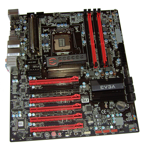
EVGA P55 FTW SLI E657
Our favorite board of the bunch for extreme benchmarking is the EVGA E657. In terms of ease of use and 'overclockability' this board wins on all counts. Our retail sample came with a TYCO AMP socket and survived everything we threw at it over the last six weeks of near 24/7 testing. At cold temperatures, this board boots up better than any other we’ve tested to date. You don’t have to boot up in safe mode or wait for temperatures to increase, it’s that simple.
Heavy load benchmarking stability is this board’s strength and at its price point there is no other P55 board that delivers on as many levels for the overclocking professional. EVGA is using TCYO AMP and LOTES sockets exclusively for all their P55 boards at this point, although there may be some early stock around still using Foxconn sockets.
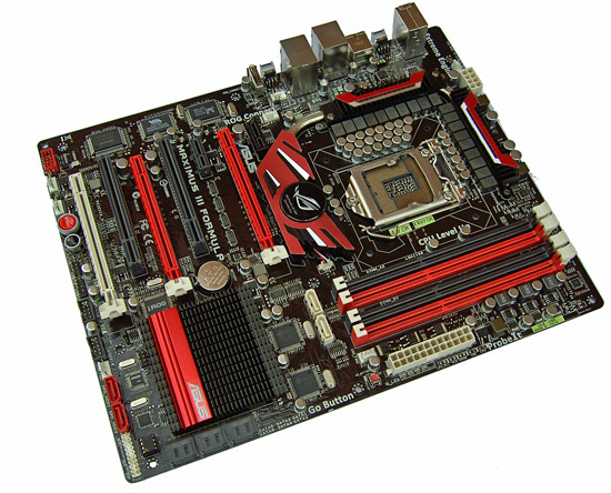
ASUS ROG Maximus III Formula
While it worked our ASUS Maximus III Formula board was a pleasure to use. In terms of overall features, BIOS design, and general desktop performance this board is rated at the top of our list. Unfortunately, the board did not respond as well as the EVGA or Gigabyte boards in extreme overclocking conditions. Our experience with the large cascade was not trouble free as it refused to post once the evaporator head temperature was below -110 degrees.
The ROG Connect software is a novel design that we see a lot of promise in and a pleasure to use as a side bonus. The board was proving itself to be the all around choice (gaming/desktop/overclocking) until we experienced the now infamous socket burn syndrome.
As of press time for this article, ASUS is still investigating the socket burnout problems and has not told us if they will be following the lead of other vendors in moving over to other socket vendors for their high end boards.
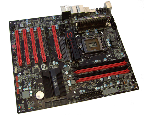
Gigabyte GA-P55- UD6
The GA-P55-UD6 from Gigabyte was on a level playing field with the ASUS ROG for the most part in general performance and extreme overclocking results. It did trail the other boards in the 8-thread CPU tests, but showed second place performance everywhere else. The UD6 handled cold temperatures as well as the E657, but required us to shut the PSU off periodically between reboots in order for the board to properly repost.
Our test sample arrived with the revised Foxconn socket and managed to survive the onslaught of benchmarks without a problem. We understand that Gigabyte has moved production over to LOTES based sockets for their higher end boards, so expect to see these showing up in the retail channels shortly.
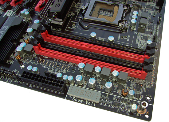
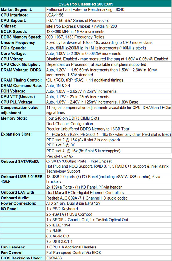
EVGA P55 Classified 200
When this board arrived in the labs we were intrigued to see what it brought to the table in comparison to less expensive P55 boards. At a $340 price point, there’s no room whatsoever for failure. Unfortunately, the only real strength that extra monetary outlay will buy you is the ability to run non-memory intensive 8-thread loads a few MHz higher than the superlative EVGA E657.
The other side bonus is for multi-GPU setups as you get dual x16 capabilities, though we wonder why you would even pick a P55 board at this price point for such a setup when there are X58 boards available to do the job better. While the board responded well in most cases, we had problems with higher memory speeds (over 2200MHz) as they were just not as stable on this board in comparison to the other boards in our tests, no matter what we tried. We’re not sure if this can be fixed without some kind of hardware change, as we tried every BIOS tweak the board has in order to try and squeeze a little more stability above DDR3-2200, but alas, no improvement.
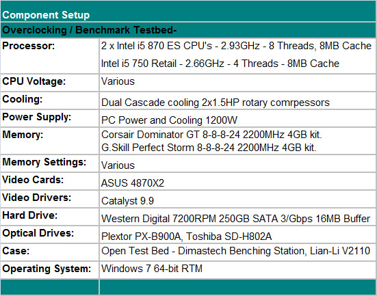
We utilize a fresh Windows 7 installation for each phase of testing to minimize variance in benchmark scores. Although Windows 7 is not ideal for benchmarks like SuperPi 32M or early 3DMarks, it does give us some indication of what is possible in terms of processor speeds on each board and allows us to utilize our normal benchmark test suite.
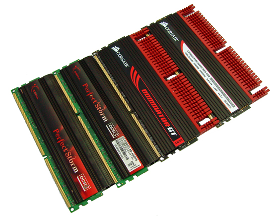
Two high-end 4GB DDR3-2200 kits from Corsair and GSkill were used throughout testing. Until our next memory review, we can safely say that the Corsair can run tighter latencies at lower voltages, while the G.Skill provides higher bandwidth capabilities on this platform. The choice of kit depends on your particular needs but either one is simply superb for overclocking. Both kits allowed us to max out the memory controllers of each test processor on all the boards we have tested to date.
3DMark Vantage
At high processor clock speeds the CPU test of 3DMark Vantage is great at weeding out board weaknesses in power delivery. Along with WPrime 1024M, this test represents one of the toughest loads these boards will be subjected to when benchmarking for scores. We used a stock clocked 4870 X2 for apples to apples comparisons of both the final score and also the maximum CPU clock we could run the entire 3D mark suite at.

The boards all fell within 50MHz of one another for outright CPU speeds. The Gigabyte board would not complete 3DMark Vantage with CPU speeds over 5GHz for us regardless of voltage changes; although the overall score per clock rate is very good. We utilized both stock memory sub-timings as set by the BIOS and then tuned each memory sub timing option. In the end, any manual changes we made did not increase stability enough to improve CPU MHz scaling the test boards.
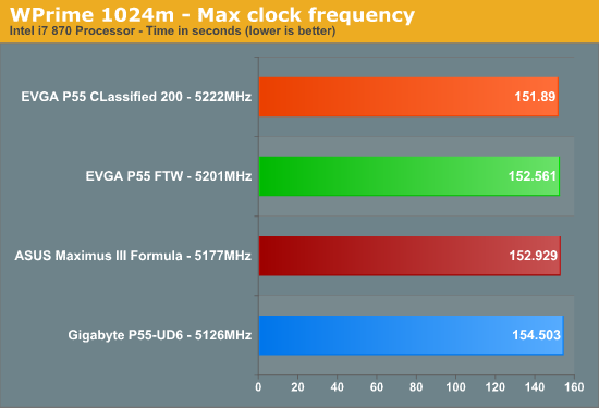
WPrime 1024M
EVGA is out in front in this bench by a small margin over the ASUS board. Surprisingly enough, the Gigabyte board would not pass WPrime 1024M on the same CPU over 5140MHz regardless of any changes we made in the BIOS. Scoring results in this long 8-thread test clearly favours EVGA due to the slight hike in raw CPU frequency.
Perhaps this should be considered a moot point given the somewhat frail nature of the i5 platform when subjected to this type of load at high processor frequencies. It’s no longer a benchmark we feel comfortable running on P55 at these types of CPU speeds due to additional stress placed on the CPU socket and processor itself. The Lynnfield/P55 is definitely a mid-range platform and as such, we highly suggest the Bloomfield/X58 platform for extreme benching if you are an Intel fan.
That being said, none of the LOTES/Tyco AMP boards suffered from socket meltdown during our testing. Also note this is the only benchmark where the EVGA E659 Classified 200 out clocked the E657 by a very slim 20MHz.
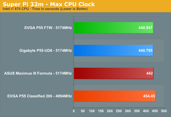
SuperPi 32M
32M is one of those benches one could waste an eternity in trying out various tweaks on both the board and in the operating systems. We decided to keep things short and simple for this review by optimizing the basic memory options and Bclk rates to show differences in how each board sets up sub-timings using the same processor and memory clocks on a given multiplier. All the boards managed the same 22x 234 BCLK using the 2:8 memory ratio.
ASUS trails by virtue of a very loose set of default sub timings. Unfortunately, we lost our ASUS ROG board to the Foxconn socket meltdown problem at this point. This also damaged our best CPU in the process so were unable to push further in this particular benchmark as our replacement processors did not clock as well.
The EVGA E659 did not fare as well as the other boards in this benchmark using the 2:10 memory ratio. No matter what we tried we could not get the board to pass 32M any higher than 226~227 BCLK in this bench. Moving over to the 2:8 ratio the E659 managed to out clock the other boards for raw CPU frequency. However, raw memory bandwidth and tight latencies favor this benchmark over the small differences in CPU frequency in our results so the lack of stability with the 2:10 memory ratio is adversely affecting the E659.
RTL -
A quick note for all you benching fanatics on the 1156/1366 platform, especially those of you that love Super Pi. ‘Round Trip Latency’ chipset function in BIOS denotes the number of Uncore Clock cycles that pass before data arrives back at the IMC after a read command is issued.
For those of you familiar with socket 775 and the P35/P45/X38/X48 chipsets, this setting is known as tRD, aka ‘Performance Level’.
‘Performance Level’ on socket 775 based processor architectures denotes the number of Front Side bus clock cycles that pass before data arrives back from the memory banks time aligned with the leading edge of a FSB clock cycle, making data transfer between the two clock domains possible.
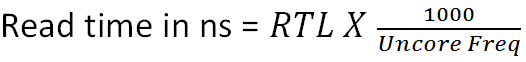
For the i5 and i7 architectures the data read time (from the time the read command was issued) can be calculated by the following formula;
Needless to say, the smaller the figure in nanoseconds, the better the performance. However, there is a change here in that although we are given control of the RTL parameter for each memory channel, the default time calculated by the memory controller at POST is almost as fast as the gearing for clock crossing can go based on aggressive timing values set by Intel.
Manual control of the RTL function has been added by board vendors to P55/X58, primarily to allow looser manual settings or to lock the setting down to a known working value. The latter is required at times because there are instances where the IMC selects a non-ideal/unstable setting for one of the memory channels, in which case locking these values down to a stable setting prevents random crashes and bizarre system instability between system reboots. Changes of 1-2 clocks below the auto-selected RTL value are sometimes possible for light load benchmarks such as a single thread of Super Pi 32M thus giving a small boost in the final time.
Socket 1156 CPU’s have their Uncore frequency multiplier locked, so there’s not too much to look out for other than a quick glance at the real RTL time in nanoseconds, to make sure that the clock crossing schedule is just as fast if not faster than your previous selected overclock.
For those of you playing around with socket 1366 processors, you get some control over the Uncore multiplier ratio (so long as you observe the minimum 2x memory multiplier rule). Bear in mind that as you increase the Uncore frequency, the RTL value will increase because more clock cycles pass over the same time period. As an example, if RTL defaults to a value of 54 clocks at an Uncore frequency of 4GHz (20x Uncore multiplier) and a memory CAS of 8, our effective read turnaround time is;

Assuming all other bus frequencies and memory timings are unchanged, if we decide to increase the Uncore Multiplier ratio to 21X, the RTL value should move out to around 57 clocks;
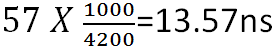
Any greater than 13.57ns, and we have lost system performance and as a double whammy will also have to increase memory controller voltage to facilitate the higher switching speed of the associated IMC stages; this is not the way to truly ‘overclock’ a system for better performance.
The reason we’re including this simple formula here is so that users can simply boot the motherboard, read the RTL value and quickly plug the numbers into the formula to work out the read time. This should help users from running repeated benchmarks for every given change in CAS and tRCD or change of a memory multiplier ratio. As always, various benchmarks will react to Uncore frequency changes in different ways, although it is handy to know if your selected operating point allows for tighter memory controller gearing than other available combinations.
We've been toying around with RTL for a few days and believe we've come up with a method of reliably predicting RTL in clocks using the following formula;
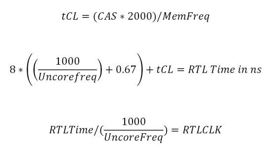
tCL denotes the True CAS Latency of the memory modules, giving us the time required to access memory at a given CAS and memory operating frequency. We take the tCL value, add it to the Uncore period we add ~670ps (approx distance to the DIMM) for each read transfer then multiply this by eight.
Do note, that the 0.67 part of the formula may need slight adjustment according to board layout; If a vendor places the DIMM slots closer to the CPU this figure will need to be reduced. You will also need to reduce this figure to around ~0.57 (570ps) for very high memory clock frequencies on some motherboards. This is because the clock skew needs to be advanced as memory clock frequency is increased. A simple Excel based calc is available if required, send me an email!
Max CPU BCLK and MHz
We used a 750 CPU for this part of the test, comparing maximum attainable BCLK using a 17x multiplier, maximum overall CPU clock validation using the same multiplier and finally the maximum Super Pi 1M pass frequency. The reason for using an i750, well, our two 870s did not survive due to the socket burn problem and before we torture our replacement processors we would like some assurances it will not happen again. As such, i750 results for the ASUS board are missing until we receive a replacement board.
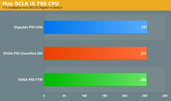
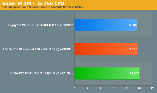
Note that using a lower CPU multiplier of 17X the Gigabyte board manages to beat the EVGA boards by 2 BCLK for outright CPU-Z validation and the EVGA P55 FTW by around 8 BCLK for Super PI 1M. At 21X however, that initial promise of higher ‘validation stable’ frequencies does not translate into higher overall overclocks even in light load benchmarks like Super Pi 1M.
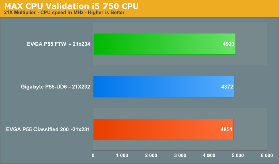
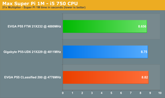
Although we managed to get a 1M to pass at 233x21 on the Gigabyte board, every time we tried to open CPU-Z to capture a screenshot, the system would crash. In the end we had to step down to 229X21 at 9-9-9-24 memory timings in order to get a screenshot with all relevant CPU tabs shown. This left us scratching our heads because at higher BCLKs using the lower CPU multipliers, the Gigabyte board showed better overall stability for validation and Super Pi 1M when pushed over 245 BCLK than the EVGA P55 FTW.
The EVGA E659 was a disappointment in this section of our testing too. Our maximum Super Pi 1M came in at 21X228 BCLK, while max validation stopped at 231 BCLK, trailing both the cheaper EVGA 657 and Gigabyte P55 UD6. This leaves the E659 as a board capable of lower stable memory speeds than the other boards in our testing with its one strength being 8-thread non-memory intensive system loads like WPrime 1024M.
Gigabyte GA-P55-UD6
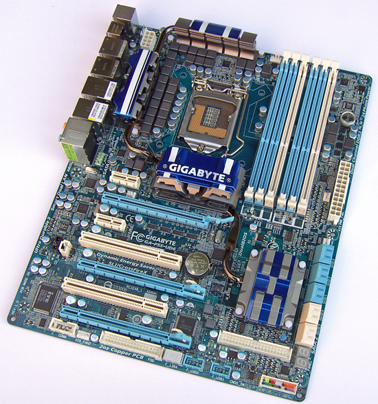
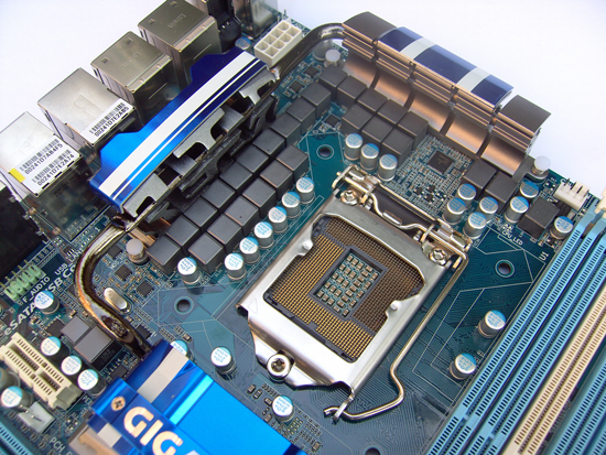
Gigabyte’s top end offering comes in at $250 and touts their answer to competing boards as having ’24-Phase’ PWM circuit (using a multiplexed ISL6336 6 phase controller). Onboard cooling of the MOSFET area, Intel P55 PCH , and Gigabyte SATA chips is provided by a heatsink/heatpipe setup connecting all three areas together. The PCH portion of the heat sink is attached with screws while the PWM MOSFETs and Gigabyte SATA chip fittings are of push-pin type (screw fittings are our favorites).
A total of 6 fan headers are available (two of which are 4 pin). Our retail sample came with a Foxconn CPU socket, although Gigabyte is moving to LOTES sockets on their upper end boards after hearing of the problems some users have experienced with the early Foxconn sockets.
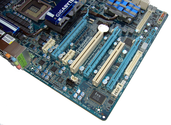
Expansion slot layout is identical to the ASUS Maximus III ROG, which is a good thing in our opinion. Starting at the top, we’ve got a PCI/eX1 slot, followed by PCI/e X16 and then another CPI/eX1 slot immediately beneath. Moving down, we get a PCI slot, the second PEG slot (running at 8X) followed by the second PCI slot and finally the last 16x mechanical PCI/e slot (running at 4x width). Slot layout is good, allowing for a variety of peripheral cards to be used in tandem. Underneath the last PCI/e slot at the lower edge of the board, we have 1XCOM port, 1XFDD, 1X1394 and 2 x USB headers.
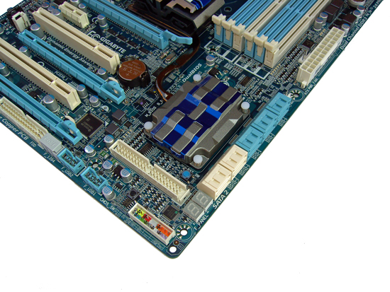
The lower right hand corner of the Gigabyte P55 UD6 is home to 10 right angled SATA ports (6 X Intel ICH10R and 4 Gigabyte SATA). A Hex post code reader is also included for debugging purposes. Just behind the Hex display, we’ve got CMOS clear and a reset switch for open test bed users. Finally an IDE port is provided for legacy drive users.
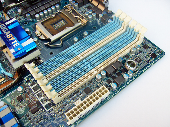
We’re a tad bemused at the presence of 6 DIMM slots on a P55 motherboard when the processors are dual channel only when run without buffered DIMMS. Oddly enough, the extra slots are for running single sided modules in dual channel interleaved mode over 6 slots. We’re not sure if this is a wise move at all because most users have moved over to double density 2GB modules which are priced attractively and capable of overclocking to high bandwidth due to advancements in memory IC design and memory controller design over previous platforms.
An onboard power button is placed very conveniently at the upper right edge of the board allowing for easy access in open test bed setups. Unfortunately, unlike the ASUS and EVGA boards, Gigabyte does not provide any voltage measurement pads for digital multimeters which can make the board a little tricky to get to grips with if you’re benchmarking under LN2.
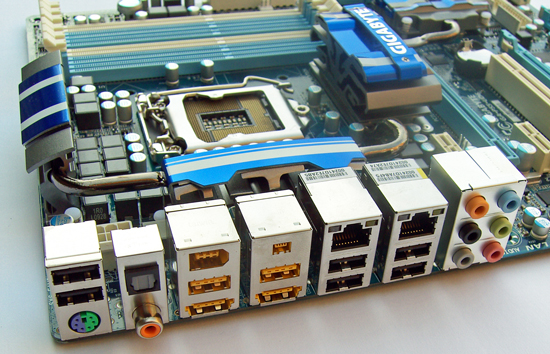
The rear panel is home to 1 x PS2, 8 x USB (2 SATA combo), 2 x1394, 1 x coaxial S/PDIF, 1 x TOSLINK optical, 2X RJ45 LAN ports and finally 6 audio output jacks. The presence of a rear CMOS clear switch would have been welcome for ease of access but is unfortunately missing. This leaves users with PC cases having to pull the side panel off their case if BIOS does not recover from a failed overclock.
Gigabyte’s Easy Tune software is bundled with the motherboard, and allows for easy access to all primary voltage rails as well as bus speed manipulation and fan control options.
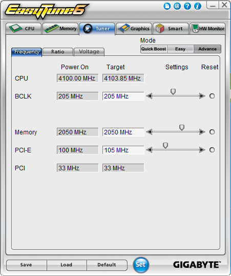
We found the Easy Tune software to be easy to use and to present a light enough system load to allow for unhindered overclocking. The only thing that would perhaps bolster Easy Tune would be the addition of hot keys with fast load profiles allowing for on the fly bus speed changes to maximize benchmark scoring potential. Other than that it’s a well rounded and easy to use tool.


EVGA P55 FTW SLI
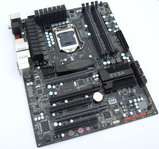
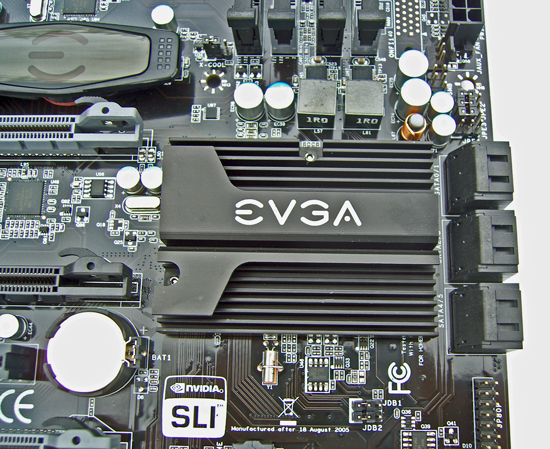
The EVGA E657 board is a little lighter in terms of onboard peripheral count when compared to the Gigabyte UD6 (additional SATA ports and software) and ASUS ROG, although the E657 FTW touts additional dedicated hardware features for overclocking (cold boot workarounds and 10 dedicated ICs allow for fine control of signal line compensation to the CPU, PCI/e and memory). CPU Power is supplied by a 12-phase, 600W capable PWM circuit, more than overkill on this platform.
A total of 7 fan headers are placed in accessible locations across the motherboard, with full fan speed control offered via BIOS. PWM cooling is catered for by two separate aluminium heat sinks that are attached to the board with screw fittings.
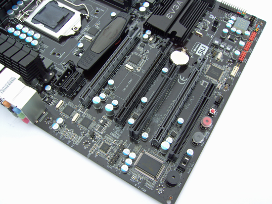
Starting at the top, expansion slot layout is comprised of PCI/eX1, PCI/e x16 (x8 if PEG slot 3 is occupied), PCI/e x4, PCI slot 1, PCI/e x8 and finally PCI slot 2.
Slot layout ensures that a PCI slot and the PCI/e x1 slots are always available/. The PCI/e x4 slot is also accessible when the primary PEG slot is occupied, although a double slot GPU will mean spacing will be tight. Underneath the last PCI slot, we find power, reset and CMOS clear buttons.
A three way slider switch is also provided allowing user selection of 3 separate BIOS IC’s. This allows flashing 3 different BIOS files, and also adds a good level of security in the instance of a corrupt BIOS flash. Along the bottom edge of the E657 we find a fan header, single IEEE-1394a connector, and three USB headers.
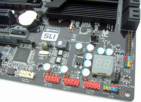
A hex post code display is placed in the lower right corner of the board and over to the left we find 3 BIOS IC’s, one of which is placed within a socket allowing removal if a swap out is required. The CFP1 connector is the EVGA OCP PCB panel connector which allows for on the fly changes 0.1V boost functions to CPU Core and VTT as well as a post code reader and power, reset and CMOS clear buttons.
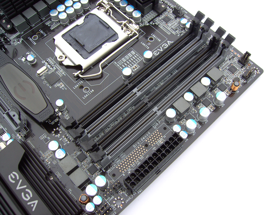
PCI/e disable and X-Cool jumpers are located underneath the DIMM slots. Memory power is supplied by a three phase controller supporting switching speeds up to 640KHz. Voltage measurement pads for all primary rails are located above the DIMM slots ensuring unhindered access in open test bed setups.
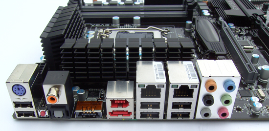
On the rear I/O panel we find, 1 x PS2, 7 X USB (1 SATA combo), 1x S/PDIF, 1x Optical, 1 x 1394, 2x RJ45 LAN and 6 x audio connectors. A CMOS reset button is located between the PS2 and S/SPDIF connectors for easy CMOS clear events with the board in a case.
Worthy of mention here is the addition of boot up voltage settings for VTT and processor Core allowing users to cold boot processors at high frequencies by applying a lower voltage during initial post.
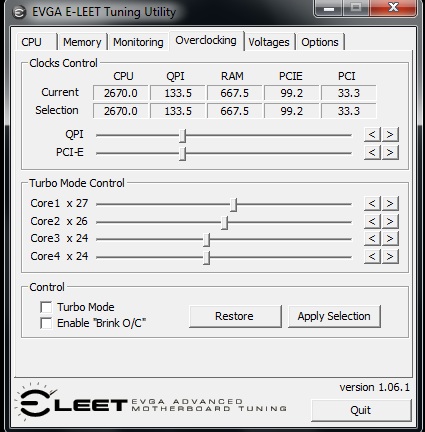
EVGA’s spin of a OS level overclocking tool know as E-LEET is also available for the P55 platform and is still the de-facto standard for all other OS overclocking tools to be judged against. ASUS’ new Connect software is close but simplicity rules here. The E-LEET GUI is remarkably compact and well laid out, offering voltage control, temperature/voltage readings, bus speed control, CPU-Z validation, quick load profiles and the ability to stop polling the SMbus. The latter feature is useful if you’d like to change processor speeds on-the-fly while minimizing the impact of having an application running in the background during a benchmark.


EVGA P55 Classified 200
EVGA’s top end offering for P55 is overkill in every single way. Classified specs add a 10-phase Volterra PWM for CPU power, a lower inductance LOTES CPU socket, an onboard digital multi-meter, and an NF200 bridge chip that adds support for triple 16x SLI or CrossFire. Like the P55 FTW E657, version 2 of EVGA’s OCP (overclocking panel) is included giving more than a subtle hint at who this board is designed for.
Priced at $340 or so, this board is more about what EVGA can do than what they should have done for this platform. The existence of X58 fills this segment with a slew of multi-gpu capable boards on the robust and higher performance socket 1366 platform. Nevertheless, we’ve added overclocking results so those who are interested can see how this board fares against others when teamed with the same components and within the same test environment.
Like the E657 model, 7 onboard fan headers are provided with full speed control via BIOS. Due to the addition of the onboard digital multi meter the E659 is classed as E-ATX with dimensions of 304.8mm X 243.8mm (LXW). This might make things a little cramped in smaller PC cases, although we think that anyone choosing a board like this is either going to be someone running an open test bed for benchmarking purposes or is someone who uses a lavish full tower PC case.
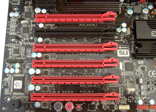
The presence of the NF200 brings a total of six 16x (mechanical) PCI/e slots and one PCI/e x1 slot to the E659. PCI/e X1 at the top, followed by the primary PEG slot running at 16x width in single GPU mode (8x when other PEG slots are occupied).For a full breakdown on lane allocation/link width check the specification table below.
No PCI slots are present on this board, which probably is not a big deal to the intended audience. Slot layout is flexible enough to cater for just about every type of configuration leaving ample upgrade room. We don’t have multi-card performance numbers at this time, although may update later if there is demand to do so.
Underneath the last PCI/e slot, we find power, reset and CMOS clear buttons. A 3 way slider switch is also provided allowing user selection of 3 separate BIOS IC’s. This allows flashing 3 different BIOS files, and also adds a good level of security in the instance of a corrupt BIOS flash. Two USB headers and a IEEE-1394a header are also placed along the bottom edge of the board.
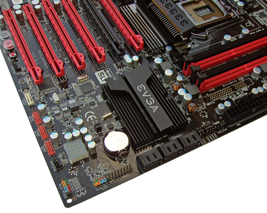
A hex post code display is placed in the lower right corner of the board and over to the left we find 3 BIOS IC’s, one of which is placed within a socket allowing removal if a swap out is required. The CFP1 connector is the EVGA OCP PCB panel connector which allows for on the fly changes 0.1V boost functions to CPU VCore and VTT as well as a post code reader and power, reset and CMOS clear buttons.
PCI/e disable and X-Cool jumpers are located underneath the DIMM slots. Memory power is supplied by a three phase controller supporting switching speeds up to 640KHz. A test lead is supplied to plug into the positive input socket of the onboard DMM. Test pads for all primary voltage rails are located above the DIMM slots.
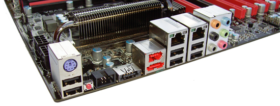
On the rear I/O panel we find 1 x PS2, 7 X USB (1 SATA combo), 1x S/PDIF, 1x Optical, 1 x 1394, 2x RJ45 LAN and 6 audio connectors. A push CMOS reset button is located between the PS2 and S/SPDIF connectors for easy CMOS clear events.
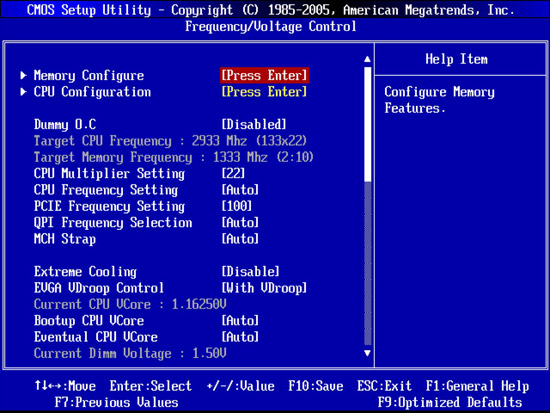
The E657 and E659 models share a practically identical BIOS (refer to screenshots on the E657 page). The only notable changes being the addition of voltage control for the added NF200 on the E659 model, together with an additional compensation adjustment for the CPU.
Final Words
We are going to keep this simple. Hold our feet to the fire and we’ll tell you that of all the boards we tested, the most consistent performer was the $230 EVGA P55 FTW SLI E657 (using a Tyco AMP Socket). At its price point, there’s nothing available on the P55 platform that truly beats it for raw overclocking capabilities. Otherwise, the ASUS Maximus III Formula was high on our list in early testing as a great overall choice until we started experiencing the socket burn problems that really plagued our review samples. We have a retail board with the revised Foxconn socket in testing now and will provide updates shortly.
The Gigabyte GA-P55-UD6 is a very good choice in the top end P55 market for those looking for a balance of features along with great overclocking abilities. We are not thrilled with the six memory sockets as it just seems to be a marketing feature. We just cannot recommend the EVGA P55 Classified 200 E659 motherboard due to its price point near $340 regardless of its capabilities, features, or even looks. Unfortunately, any jubilation for a platform winner ends here until we know the exact cause of the issues we experienced on motherboards using the Foxconn 1156 sockets.
Behind the scenes, Foxconn admitted there was a socket update in June that was approved by Intel with planned implementation in the August time period. We have the test report papers and the revised Foxconn socket passed all of Intel’s stress tests before it was placed into production, which raises questions as to why there has been problems post retail release. Intel has only commented that they believe the problems can occur with improper force being placed on the socket. However, that does not explain the lack of pad contacts with a retail CPU cooler and new processor that we have experienced in several situations.
Whether the reported socket issues were down to poor contact, improper clamp force, or a limitation in design (limited tolerances beyond stock specifications) is unknown to us at present. We’ve spoken to a few board engineers and nobody has been able or willing to put a firm conclusion on the matter, at least on the record.
Off record, early results from failed boards or user reports appeared to be a serious enough problem that most of the manufacturers moved to the Lotes or Tyco AMP sockets in their high-end boards or others for that matter. We have to stress that our problems and those of others we have dealt with directly occurred under extreme overclocking conditions. Out on the forums, we’ve heard of one reported case where a user claims a failure has happened at stock operating frequency using an Intel air cooler. We also have verification of a Lotes socket failing recently, which does put a new light on this problem.
Socket issues aside, the margin of overclocking variance shown in our benchmark results are very small. We can assure you that any of these clock speed differences won’t show up when these boards are used with air or water cooling solutions. And even with the socket burn out problems, we just have not had any direct experiences with failures after close to nine thousand test hours on over a dozen retail boards with air or water cooling at this point. Based on that testing, we still feel confident about the P55 platform.
For the sub-zero benchmarking crowd, you’re not likely to upstage socket 1366 based processors by using any kind of budget purchasing angle with the P55 platform. Just be aware and realistic of what this platform is designed to do before you commit to purchase it with thoughts of setting overclocking records in mind.
Gallery of Additional Performance Results-


