Original Link: https://www.anandtech.com/show/2679
The RV770 Story: Documenting ATI's Road to Success
by Anand Lal Shimpi on December 2, 2008 12:00 AM EST- Posted in
- GPUs
This was the email that set it off:
Hi Anand,
You have an appointment with Carrell Killebrew at 3pm tomorrow at ATI Santa Clara - he's going to give you the background on what REALLY went on behind 770. He'll meet you in the lobby on the 5th floor.
Chris
The email was from Chris Hook, PR at AMD, I’d worked with him for years and at ATI before the acquisition. I’ve always given him a hard time for trying to spin me, for doing a great job of hosting parties but a terrible job of putting me face to face with the brightest engineers.

Chris Hook seems terribly uninterested in whatever is coming out of my mouth at this dinner years ago :)
Lately Chris has been on a quest to prove me wrong. He gets that I don’t care about the parties or the exotic destinations that AMD usually hosts its press events at, I just want the product and the engineers. Earlier this year Chris let one engineer out of the bag and we had a great conversation about AMD’s manufacturing and packaging technologies (yeah, I’m a boring date). He gained a bit of trust with that interaction, so when he sent me the email above my ears perked.
I made my way back to ATI Santa Clara for the 3PM meeting and as I exited the elevator I heard “Anand?” from behind me. I didn’t recognize any of the men there but that’s not too unusual, in my old age remembering all of the faces is getting difficult, after all I’ve been doing this for nearly 12 years now. Thankfully this wasn’t one of those cases of forgotten identities, the man who I’d soon find out was Carrell Killebrew simply recognized me from a picture. What picture? I have no idea, perhaps AMD keeps pictures of Derek, Gary and myself on walls to know who to be angry at.
We walked around 30 feet into a small room with a table and some chairs, there was a speakerphone in the middle of the table. In the room was myself, Carrell Killebrew, Eric Demers, Mike Schmit and Mark Leather.
Most of these people I’d never met before, although I had heard their names. AMD, and ATI before the acquisition, had historically done a terrible job of giving us access to their smartest people. At best we’d get people in technical marketing, but very rarely the lead architects or any Fellows (read: certified genius title). That day however, on my day off, I found myself in a room with AMD Fellow after Fellow, smart guy after smart guy...and not a single member of AMD PR to muzzle the engineers.
To appreciate Carrell you have to understand that most of the people we talk to about GPUs are there to market us, and do so in a very markety tone. These briefings normally start out with some slides on the lay of the land, talking about how gaming is important, then there’s some architecture talk, a bit about the cards, some performance data that we don’t pay attention to and then a couple of conclusion slides. For a company that builds products that let you blow off peoples’ heads and watch the whole thing in greater fidelity, the way they talk to us about product is pretty lame.
Carrell, was different. Carrell Killebrew was the engineering lead on RV770, the GPU behind the Radeon HD 4800 series, and he was exactly the type of person you’d expect to be lead engineer on a product used to play video games, ridiculously fun, video games.
Carrell started the conversation off by saying that everything he was about to tell me would be on record, and he was assuming that no one had any objections to that. This was going to be good.
He asked me what I’d like to talk about and he offered some choices. We could talk about future GPU trends and architectures, we could talk about GPU accelerated video transcoding or he, along with the rest of the group, could give me the back story on RV770.
Carrell’s final option piqued my interest, I hadn’t really thought about it. When RV770 launched in the summer we took for granted that it was a great part, it upset NVIDIA’s pricing structure and gave us value at $200 and $300. We went through the architecture of the Radeon HD 4800 series and looked at performance, but I spent only a page or so talking about AMD’s small-die strategy that ultimately resulted in the RV770 GPU. AMD had spent much of the past 8 years building bigger and bigger GPUs yet with the RV770 AMD reversed the trend, and I didn’t even catch it. I casually mentioned it, talked about how it was a different approach than the one NVIDIA took, but I didn’t dig deeper.
Normally when a manufacturer like AMD tells me they did something, I ask why. When Intel introduced me to Nehalem’s cache architecture, I asked why and later published my findings. And for the most part, with every aspect of the Radeon HD 4800’s architecture, we did the same. Derek Wilson and I spent several hours on the phone and in emails back and forth with AMD trying to wrap our heads around the RV770’s architecture so that we could do it justice in our reviews. But both of us all but ignored the biggest part of RV770: the decision that led to making GPU itself.
This is a tough article for me to write, there are no graphs, no charts, no architecture to analyze. I simply got to sit in that room and listen as these individuals, these engineers shared with me over the course of two hours the past three years of their lives. I want to do it justice, and I hope that I can, because what they conveyed to me in that room was the best meeting I’d ever had with AMD or ATI.
The Beginning: The Shot Heard Around the World
It all started back in 2001 when ATI, independent at the time, was working on the R300 GPU (Radeon 9700 Pro). If you were following the industry at all back then, you’d never forget the R300. NVIDIA was steadily gaining steam and nothing ATI could do was enough to dethrone the king. The original Radeon was a nice attempt but poor drivers and no real performance advantage kept NVIDIA customers loyal. The Radeon 8500 wasn’t good at all; there was just no beating NVIDIA’s GeForce4, the Ti 4200 did well in the mainstream market and the Ti 4600 was king of the high end.
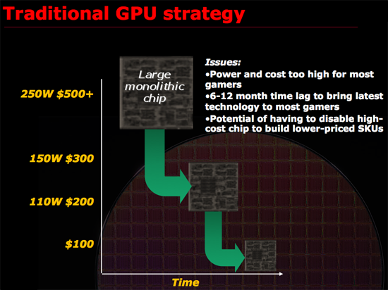
While ATI was taking punches with the original Radeon and Radeon 8500, internally the company decided that in order to win the market - it had to win the halo. If ATI could produce the fastest GPU, it would get the brand recognition and loyalty necessary to not only sell those high end GPUs but also lower end models at cheaper price points. The GPU would hit the high end first, but within the next 6 - 12 months we’d see derivatives for lower market segments. One important takeaway is that at this point, the high end of the market was $399 - keep that in mind.
With everyone at ATI thinking that they had to make the fastest GPU in the world in order to beat NVIDIA, the successor to the Radeon 8500 was going to be a big GPU. The Radeon 8500 was built on a 0.15-micron manufacturing process and had around 60M transistors; R300 was going to be built on the same process, but with 110M transistors - nearly twice that of the 8500 without a die shrink.
Its competition, the GeForce4 was still only a 63M transistor chip and even NVIDIA didn’t dare to build something so big on the 150nm node, the GF4 successor would wait for 130nm.
We all know how the story unfolded from here. The R300 was eventually branded the ATI Radeon 9700 Pro and mopped the floor with the GeForce4. What Intel did to AMD with Conroe, ATI did to NVIDIA with R300 - back in 2002.
The success with R300 solidified ATI’s strategy: in order to beat NVIDIA, it had to keep pushing the envelope for chip size. Each subsequent GPU would have to be bigger and faster at the high end. Begun these GPU wars had.
Re-evaluating Strategy, Creating the RV770 in 2005
Remembering what lead to success rather than the success itself is generally more important, and around 2005 ATI had another R300 moment. What made R300 successful was ATI re-evaluating the way it made GPUs and deciding on something that made sense. At the time, it made sense for ATI to work towards building the biggest chip possible, win at the high end and translate that into better, more competitive products at all other price points. It is worth mentioning that part of R300’s continued success was due to the fact that NVIDIA slipped up royally with the GeForce FX, it was the perfect storm and ATI capitalized. ATI built the biggest chip and NVIDIA had no real answer for some time to come.
Just as Intel bumped into the power wall when it tried to ramp Pentium 4 clock speeds to ridiculous levels, ATI was noticing that GPUs were getting a little too big for comfort. Design cycles were getting longer, die size was growing and financially there were some things that didn’t quite make sense when it came to making these large GPUs.
ATI asserted that a very large GPU, without the use of repair structures or harvesting (two techniques I’ll describe in a bit) may only have a 30% yield. That means for every 100 GPUs produced on a single wafer, only 30% of them would be fully functional and could be sold as advertised. Manufacturing these complex circuits is particularly expensive, those fab plants easily cost a couple of billion dollars to build and thus having most of your wafer go to waste isn’t really a good way of running a business.
Thankfully there are ways to improve that crappy 30% yield to a value north of 90%. The first is a technique generally known as repairability. The idea behind repairability is simple: build redundancy into your design. If you have a unit with 10 shader processors, actually build 11 but use one as a spare should there be a defect in any of the remaining processors. The same technique is often used for on-die memory, include additional cells so that a defect in one part of a cache won’t render the entire chip unusable. There are tradeoffs here however, if you build in too much repairability then you run the risk of having a die that’s large but offers no additional performance benefit. If you don’t build in enough repairability then your yield suffers.
Harvesting is another technique that all of you are quite familiar with, although its street name is feature binning. The idea here is that you assume that only a small percentage of the die on a wafer will be completely functional, but instead of throwing away the ones that aren’t fully functional, you disable features and sell them as a lower end part. For example, if your target architecture has 10 shader processors but only 30% of your production will have 10 working shader processors but 50% of the production will have 8 working units you’d sell a model with 10 SPs and a model with 8 SPs, the latter being at a reduced cost. This way instead of throwing away 70% of the wafer, you only throw away 20% - and if possible you could make a third SKU with fewer number of functional SPs and use close to 100% of the wafer.
Yields do improve over time, and what eventually happens if you build a product relying on harvesting is you hurt yourself financially. In the example above where you have two configurations of the same die, yields will eventually improve to the point where your 8 SP die could just as easily have 10 functional SPs but you have to sell them as reduced functionality parts because you’ve built up market demand for them. In a sense, you’re selling something worth $1 for $0.80. You could always create a new version of the chip with a smaller die, but that takes additional engineering resources, time and money.
The most recent public example of die harvesting was actually with NVIDIA’s GT200. The GeForce GTX 260 was simply a harvested version of the GTX 280 with 192 SPs vs. 240. As yields improved, NVIDIA introduced the GeForce GTX 260 Core 216 with 216 SPs. Note that NVIDIA didn’t use any repairability for the shader processors on GT200 there are no more than 240 functional SPs on a GT200 die, but that’s because NVIDIA would rely on harvesting anyway - if any of the 240 SPs didn’t work the chip would be branded as a GTX 260 or Core 216.
This is in stark contrast to RV770 where both versions of the GPU were functionally identical, the only differences were clock speeds and power requirements. But from a die standpoint, ATI didn’t have to sell any reduced versions of the chip to keep yields high.
Note that whether or not a company has to rely on harvesting doesn’t really impact the end user. In this case, the GeForce GTX 260 Core 216 actually benefitted the end user as it manages to deliver the same sort of value that AMD does with the Radeon HD 4870. It isn’t ideal for NVIDIA financially and if a company has to rely on harvesting for too long it will eventually take its toll, but I suspect that in the GT200 case NVIDIA will bail itself out with a 55nm revision of GT200 before things get too bad.
ATI didn’t want to build a GPU that would rely on excessive repair and harvesting to keep yields high. And then came the killer argument: building such a GPU was no longer in the best interests of its customers.
Sidenote: Building a GPU
Before we get too far down the rabbit hole it’s worth adding some perspective. ATI’s RV770 design took three years of work, that means ATI started in 2005. It takes about a year for manufacturability from tapeout to final product ship, another 1 - 1.5 years for design and another year for architecture.
The team that I met with in Santa Clara was talking about designs that would be out in 2012, we’re talking 4 TFLOPS of performance here, 4x the speed of RV770.
Decisions being made today are going to impact those products and in a sense it’s a big guessing game, ATI has no idea what NVIDIA will have in 2012 and NVIDIA has no idea what ATI will have. Each company simply tries to do the best it can for the customers and hopes they’ve got the right mix of performance, price and power.
To give you an idea of the intensity of some of these debates, Carrell debated, every evening, for three hours, for three weeks, the amount of repairability that would go into the RV770. Building redundant structures in the RV770 was an even bigger deal than before because ATI was going to be working within serious die constraints, simply making the chip bigger wasn’t an option. Repair structures in the RV770 wouldn’t add any performance but would increase the die size, on an already large chip that’s fine, but on a chip that’s supposed to target the sweet spot and can’t grow without limit it’s a big deal.
Building a GPU for the Masses
AMD put up this graph at its recent Financial Analyst Day:
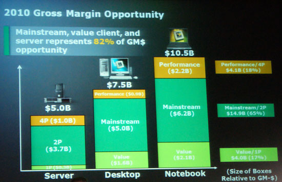
The performance segment of the desktop CPU market is only about 7% of the pie and although it generates a disproportionately large amount of revenue it’s neither the biggest segment nor the biggest revenue generator in the market. That would be the mainstream segment.
ATI realized much of the same thing back in 2005. These high end GPUs were getting more and more expensive, while R300 tipped the scales at $399 over the coming years we’d see GPUs hit $499, $599 and go north of $600 at launch. The higher prices were due to increasing die sizes and techniques such as harvesting, ensuring that regardless of how big the GPU, revenues were protected.
A $399 R300 was close enough to the mainstream price points that ATI was able to scale it down months later to address other markets, but these days the time between the high end GPU introduction and the mainstream revisions of it has increased to 6 - 9 months. We still don’t have a mainstream derivative of NVIDIA’s GT200 architecture and chances are that we won’t until around 9 months after its introduction. With the GeForce GTX 280 launching at $600, for it to take 9 months to make a $200 derivative is doing the market a disservice in ATI’s eyes.
It was time to refocus. Instead of tailoring to the needs of the high end, ATI wanted to make a product that would be the best in the $200 - $300 range. To do so would mean that it would have to reverse the strategy that made it successful to begin with, and hope that somehow NVIDIA wouldn’t follow suit.
The Bet, Would NVIDIA Take It?
In the Spring of 2005 ATI had R480 on the market (Radeon X850 series), a 130nm chip that was a mild improvement over R420 another 130nm chip (Radeon X800 series). The R420 to 480 transition is an important one because it’s these sorts of trends that NVIDIA would look at to predict ATI’s future actions.
ATI was still trying to work through execution on the R520, which was the Radeon X1800, but as you may remember that part was delayed. ATI was having a problem with the chip at the time, with a particular piece of IP. The R520 delay ended up causing a ripple that affected everything in the pipeline, including the R600 which itself was delayed for other reasons as well.
When ATI looked at the R520 in particular it was a big chip and it didn’t look like it got good bang for the buck, so ATI made a change in architecture going from the R520 to the R580 that was unexpected: it broke the 1:1:1:1 ratio.
The R520 had a 1:1:1:1 ratio of ALUs:texture units:color units:z units, but in the R580 ATI varied this relationship to be a 3:1:1:1. Increasing arithmetic power without increasing texture/memory capabilities; ATI noticed that shading complexity of applications went up but bandwidth requirements didn’t, justifying the architectural shift.
This made the R520 to R580 transition a much larger one than anyone would’ve expected, including NVIDIA. While the Radeon X1800 wasn’t really competitive (partially due to its delay, but also due to how good G70 was), the Radeon X1900 put ATI on top for a while. It was an unexpected move that undoubtedly ruffled feathers at NVIDIA. Used to being on top, NVIDIA doesn’t exactly like it when ATI takes its place.
Inside ATI, Carrell made a bet. He bet that NVIDIA would underestimate R580, that it would look at what ATI did with R480 and expect that R580 would be similar in vain. He bet that NVIDIA would be surprised by R580 and the chip to follow G70 would be huge, NVIDIA wouldn’t want to lose again, G80 would be a monster.
ATI had hoped to ship the R520 in early summer 2005, it ended up shipping in October, almost 6 months later and as I already mentioned, it delayed the whole stack. The negative ripple effect made it all the way into the R600 family. ATI speculated that NVIDIA would design its next part (G71, 7900 GTX) to be around 20% faster than R520 and not expect much out of R580.
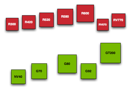
A comparison of die sizes for ATI and NVIDIA GPUs over the year, these boxes are to scale. Red is ATI, Green is NV.
ATI was planning the R600 at the time and knew it was going to be big; it started at 18mm x 18mm, then 19, then 20. Engineers kept asking Carrell, “do you think their chip is going to be bigger than this?”. “Definitely! They aren’t going to lose, after the 580 they aren’t going to lose”. Whether or not G80’s size and power was a direct result of ATI getting too good with R580 is up for debate, I’m sure NVIDIA will argue that it was by design and had nothing to do with ATI, and obviously we know where ATI stands, but the fact of the matter is that Carrell’s prediction was correct - the next generation after G70 was going to be a huge chip.
If ATI was responsible, even in part, for NVIDIA’s G80 (GeForce 8800 GTX) being as good as it was then ATI ensured its own demise. Not only was G80 good, but R600 was late, very late. Still impacted by the R520 delay, R600 had a serious problem with its AA resolve hardware that took a while to work through and ended up being a part that wasn’t very competitive. Not only was G80 very good, but without AA resolve hardware the R600 had an even tougher time competing. ATI had lost the halo, ATI’s biggest chip ever couldn’t compete with NVIDIA’s big chip and for the next year ATI’s revenues and marketshare would suffer. While this was going on, Carrell was still trying to convince everyone working on the RV770 that they were doing the right thing, that winning the halo didn’t matter...just as ATI was suffering from not winning the halo. He must’ve sounded like a lunatic at the time.
When Carrell and crew were specing the RV770 the prediction was that not only would it be good against similarly sized chips, but it would be competitive because NVIDIA would still be in overshoot mode after G80. Carrell believed that whatever followed G80 would be huge and that RV770 would have an advantage because NVIDIA would have to charge a lot for this chip.
Carrell and the rest of ATI were in for the surprise of their lives...
If it Ain’t Broke...
The status quo is a dangerous thing. In 2005 ATI and NVIDIA were both sitting on a formula that worked: build the fastest GPU in the world (and provide solid drivers), and you’d win the market. By this point ATI had years of support to continue building GPUs this way, but there were a few within the company who believed it was time for a change.
In many ways ATI and NVIDIA were just taking different risks. NVIDIA had learned its lesson with transitioning to new manufacturing processes too quickly and would most likely build GT200 on an older, more mature process, burdening it with a huge die. ATI opted to do what NVIDIA wouldn’t and move to new manufacturing processes quicker, aiding it in producing GPUs with smaller dies.
With its only competitor hell bent on making bigger and bigger GPUs, ATI took care of half of the problem - it would be free to do whatever it’d like, without any real competition. The question then became - could it work?
It’s easy to, today, look back and say “of course” but you have to understand that this was 2005 and the first specifications of RV770 were being drafted. Imagine sitting at a table full of people whose jobs were supported by building the biggest GPUs in the world and suggesting that perhaps we sit this round out. Let NVIDIA take the crown, let them have the halo part, we’ll compete in the $200 - $300 market. Yeah, right.
What followed were heated debates, if ATI were to stake the future of its graphics business on not building the absolute faster GPU, but rather a GPU targeted at a lower market segment the proposition was risky.
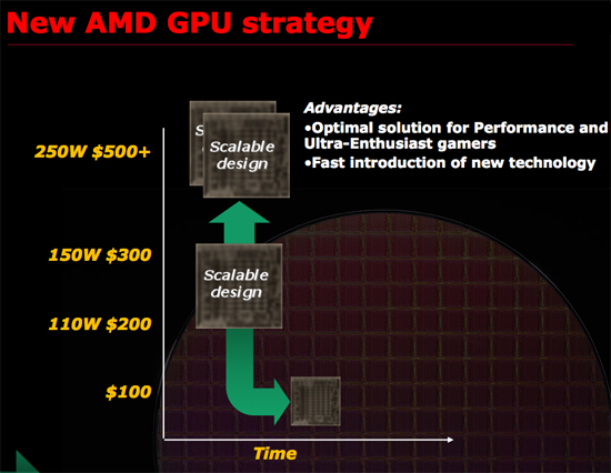
ATI viewed the graphics market as five segments: Enthusiast, Performance, Balance, Mainstream and Value. In the Spring of 2005, ATI decided to shoot for the Performance segment, and not Enthusiast. You could even argue that the Performance segment is what the R300 competed in back in 2002, priced at $399 it was closer to the $299 MSRP of the Radeon HD 4870 than the $599 MSRP of the GeForce GTX 280 when it launched. But ATI viewed this as a change in strategy, while R300 aimed for performance regardless of die size, RV770 would have clear power and die size limits imposed on it.
There were many individuals at ATI that were responsible for the RV770 we know today getting green lighted. ATI’s Rick Bergman was willing to put himself and his career on the line, because if this didn’t work, he’d be one to blame. Carrell recalled a story where Rick Bergman and others were at a table discussing RV770; Rick turned to Matt Skynner and asked him if he thought they could really do it, if they could make RV770 a smaller-than-NVIDIA GPU and still be successful, if it was possible to create a halo in the Performance segment. Matt apparently pondered the question, turned to Rick and said “I think we can”. Carrell felt that ATI might not have gone down that path if it weren’t for Matt Skynner’s support and Rick Bergman making sure that the project was executed as well as it ended up being.
It was far from rosy at that point however, there were many very smart engineers, people who were responsible for things like R300 and R580 who disagreed with the strategy. People who had been right before were saying that if ATI didn’t build a true competitor to GT200 that the fight would be over. Then you had folks like Carrell saying that it could be done, that this was absolutely the right move. It’s much like the passion of politics, each side believed that they were right, but ultimately you can only pick one - and both sides have to live under the same roof.
Depression Sets in but the Team Goes On
The entire RV770 design took around three years, which means that while we were beating ATI up over the failure that was R600, those very engineers had to go into work and be positive about RV770. And it was tough to, after all ATI had just completely lost the crown with R600 and Carrell, Rick Bergman and others were asking the team to ignore what happened with R600, ignore the fact that they lost the halo, and try to build a GPU that aimed at a lower market segment.
Through all of my interviews, the one thing that kept coming up was how impressed ATI was with the 770 team - never once did the team fall apart, despite disagreements, despite a shaky direction, the team powered through.
The decision not to go for the king of the hill part was a decision that made a lot of sense with ATI, but there was so much history about what would happen if you didn’t get the halo part; it took a very strong discipline to cast history aside and do what the leads felt was right, but the team did it without question.
The discipline required wasn’t just to ignore history, but to also fight the natural tendency for chips to grow without limits during their design phase. What ATI achieved with RV770 reminded me a lot of Intel’s Atom design team, each member of that team had strict limits on how big their blocks could be and those limits didn’t waver.
Adversity tends to bring the best out of people. The best stories I’ve been told in this industry, the Intel folks who made Banias and the ATIers that were responsible for RV770 put their hearts and souls into their work, despite being beat down. Passion has a funny way of being a person’s strongest ally.
The Power Paradigm
We were all guilty for partaking in the free lunch. Intel designed nearly five years of processors without any concern for power consumption and the GPU guys were no different.
In the R300 and R420 days ATI was almost entirely ignoring power, since estimating how much power the parts would use was so off from the final product that they just didn’t care. It was such a non-issue in those days that ATI didn’t even have a good way to estimate power even if it wanted to, it was impossible to design for a specific TDP. Today ATI’s tools are a lot better, now targeting a specific TDP is no different than aiming for a specific clock speed or die size, it’s another variable that can now be controlled.
These days power doesn’t change much, the thermal envelopes that were carved out over the past couple of years are pretty much stationary (ever wonder why the high end CPUs always fall around 130W?). Everyone designs up to their power envelope and stays there. What matters now is every year or two increasing performance while staying within the same power budget. Our processors, both CPUs and GPUs, are getting more athletic, rather than just putting on pounds to be able to lift more weight.
One of the more interesting things about architecting for power is that simply moving data around these ~1 billion transistor chips takes up a lot of power. Carrell told me that by the time ATI is at 45nm and 32nm, it will take as much power to move the data to the FPU as it does to do the multiply.
Given that data movement is an increasingly power hungry task a big focus going forward is going to be keeping data local when possible, minimizing moving to registers and on-chip caches. We may see more local register files and more multi-tiered memory hierarchies. As chips get more complex, keeping the register file in one central location becomes a problem.
ATI admitted to making a key manufacturing mistake with R600. The transistor technology selected for R600 was performance focused, designed to reach high clock speeds and yielded a part that didn’t have good performance per watt - something we noticed in our review. ATI has since refocused somewhat away from the bleeding edge and now opts for more power efficiency within a given transistor node. With leakage a growing problem as you go to smaller transistors it’s not worth it to be super leaky to gain a few picoseconds. If you’ve got a 100W GPU, do you want to waste 40W of that budget on leakage? Or would you rather do 80W of real work and only waste 20W? It’s the same realization that Intel recognized during the Pentium 4’s term and it’s the mentality that gave us the Core microarchitecture. It’s an approach that just makes sense.
Just One Small Problem: We Need a New Memory Technology
The R600 GPU had an incredibly wide 512-bit memory interface, the problem with such a large interface is that it artificially makes your die bigger as you’ve got to route those interface pads to the memory devices on the board. For RV770 to have the die size ATI wanted, it needed to have a 256-bit memory interface, but using (at the time) current memory technology that wouldn’t give the GPU enough memory bandwidth to hit the performance targets ATI wanted.
When the options were either make the chip too big or make the performance too low, ATI looked elsewhere: let’s use a new memory technology. Again, put yourself in ATI’s shoes, the time was 2005 and ATI had just decided to completely throw away the past few years of how-to-win-the-GPU-race and on top of that, even if the strategy were to succeed it would depend on a memory technology that hadn't even been prototyped yet.
The spec wasn’t finalized for GDDR5 at the time, there were no test devices, no interface design, nothing. Just an idea that at some point, there would be memory that could offer twice the bandwidth per pin of GDDR3, which would give ATI the bandwidth of a 512-bit bus, but with a physical 256-bit bus. It’s exactly what ATI needed, so it’s exactly what ATI decided to go with.
Unfortunately whether or not GDDR5 shipped by the summer of 2008 wasn’t all up to ATI, the memory manufacturers themselves had a lot of work to do. ATI committed a lot of resources both monetarily and engineering to working with its memory partners to make sure that not only was the spec ready, but that memory was ready, performing well and available by the summer of 2008. Note that the RV770 was going to be the only GPU that would use GDDR5, meaning that it was ATI and ATI alone driving the accelerated roadmap for this memory technology. It’s akin to you trying to single handedly bring 100Mbps internet to your city; it’ll happen eventually, but if you want it done on your time table you’re going to have to pickup a shovel and start burying a lot of your own cable.
ATI did much of the heavy lifting with the move to GDDR5, and it was risky because even if RV770 worked out perfectly but the memory wasn’t ready in time the GPU would get delayed. RV770 was married to GDDR5 memory, there was no other option, if in three years GDDR5 didn’t ship or had problems, then ATI would not only have no high end GPU, but it would have no performance GPU to sell into the market.
If GDDR5 did work out, then it meant that RV770 could succeed and that it would be another thing that NVIDIA didn’t have at launch. That is, of course, assuming that ATI’s smaller-die strategy would actually work...
Dave Baumann Saves the Radeon HD 4850
ATI had this habit of finding good reviewers and bringing them on staff. Our first Graphics Editor, Matthew Witheiler, went to work for ATI after graduating from Duke. He was with AnandTech for a good three years before ATI snagged him, he ended up being ATI’s youngest Product Manager (congrats on the engagement Matthew). One other prominent reviewer ATI grabbed ahold of was Dave Baumann of Beyond3D fame and brought him on to do technical marketing.
One of Baumann’s strongpoints was the ability to analyze the competitive landscape given that’s what he did for Beyond3D before ATI. One of Dave’s first major tasks at ATI was to compare R600 to G80 internally, which wasn’t exactly the best job in November of 2006. Obviously, G80 had a significant impact on RV770. While the architecture was set in stone, clock speeds, board layout and memory sizes were all variable until early 2008.
Initially, RV770 was targeted at 1.5x the performance of R600, which looking back would not have been enough. During the next 1.5 years that 1.5x turned into 2x R600 and finally settled at 2.5x the speed of R600, at a price in the $200 - $300 range.
Dave became a product manager on RV770 by February 2008, which was a big deal given that he hadn’t been with ATI that long and this was a very important product. RV670 saw ATI return to competition in the year prior, but RV770 needed to put ATI back on top.
When Dave took the 770 under his wing a lot of the product had already been mapped out, the chip was back from the fabs and at this point ATI’s engineering team wasn’t ready or eager to make any changes. The RV770 XT sat well with Mr. Baumann (the XT was the internal name of the Radeon HD 4870), in his words “the specifications were perfect”. There was a late change to the 4870 that gave it its second PCIe power connector, but that’s it. Arguably the more important version, the RV770 Pro that would become the Radeon HD 4850, concerned him - it was a bit under spec’d.
Here’s a quick put-yourself-in-ATI’s-shoes test. Your engineering team has spent the past three years on a product that may fail miserably because it’s a radical departure from how you’ve designed GPUs in the past. Your last major GPU architecture launch failed miserably (R600), and the last refresh (RV670) did ok but still didn’t really snag real mindshare from NVIDIA. You’ve just finished this radical new design, and this young new PM with an accent comes in three months before you’re supposed to enter production and tells you that you need to make changes. It was a ballsy move by Baumann, but he wasn’t interested in saving face, he was trying to help his team win. The engineers could’ve just as easily cast him aside, but they listened and they worked, oh did they work. The final stretch is rarely the quickest or the easiest, and this is very true about RV770.
The Radeon HD 4850 was originally a 256MB card with a 500MHz core clock and 900MHz memory clock. Dave insisted that the card needed 512MB of GDDR3 and 625MHz core / 993MHz memory clock, it’s not just that he insisted, but that he convinced the engineers to make such a late change. Dave took the engineers through his reasoning of why and where ATI needed to be in the competitive landscape, by the end of the discussion he didn’t need to persuade them, the board and ASIC teams were championing the changes.
Had it not been for these modifications, the 4850 would not have put as much pressure on NVIDIA’s GeForce 9800 GTX and its pricing wouldn’t have needed to fall so quickly.
Thanks Dave.
The Last Hiccup: Boards Went on Sale Too Soon
The RV770 products were finished in May of 2008, production started by June. Even up until the day that the embargo lifted there were some within ATI who felt they had made a mistake with the smaller-die strategy, but they were going to find out how right the strategy was, even sooner than expected.
The last bump in the road to the Radeon HD 4800 came just a week before launch. We had literally just gotten our first Radeon HD 4850 cards when Chris Hook called and told me that some 4850s had started selling in Europe.
In order to salvage the launch ATI was proposing the following: we could talk about Radeon HD 4850 performance, but we couldn’t talk about the 4870 or the RV770 architecture.
Within 30 hours we had our first preview up and made it already clear that ATI was on to something. The GeForce 9800 GTX got an abrupt price drop to remain competitive and even then it wasn’t enough, the Radeon HD 4850 was the card to get at $199.
The last hiccup in ATI’s launch ended up not being bad at all, ATI got some extra PR, drummed up some added excitement and in the end did justice to a product that deserved it.
Recon from Taiwan
One thing I wondered was how well ATI knew NVIDIA’s plans and vice versa, so I asked the obvious: where do you guys get your information from? The answer was pretty much as expected: Taiwan. All of the board makers know one another and are generally open with sharing information, once information hits Taiwan it’s up for grabs. Then there’s a bit of guesswork that’s done.
ATI planned to put its best foot forward, looking at the roadmaps it seemed like NVIDIA wasn’t going to do much in the G92 space in the time period that ATI would launch RV770. NVIDIA had its sights set on another G80-esque launch with GT200, it would introduce this honkin new chip, price it out of the reach of most and not worry about the peasants until sometime in 2010. The existing product line would be relied on to keep the masses at bay.
ATI was lucky that NVIDIA only had GT200 for the end of 2008 and that NVIDIA’s GT200 performance wasn’t exactly where it needed to be, because it created an opportunity that ATI has only had a couple of times in the past decade.
With the Radeon HD 4850 the initial goal was to make a product that was certainly better than the 8800 GT. It was never a goal for the 4850 to be competitive with the 9800 GTX, after all that was a $300 part and this would sell for $200.
The Radeon HD 4870 was targeted to be faster than the 9800 GTX, which again would make a lot of sense since this was ATI’s $300 part and the GTX was NVIDIA’s. What ATI didn’t expect was for the 4870 to do so well against the GeForce GTX 260. When NVIDIA finally launched the GeForce GTX 280/260 ATI looked at the results and let out a collective “wait a minute”. It worked out perfectly, not only did ATI hit the competitive points it wanted to but thanks to GT200 performance being lower than ATI expected and the RV770 doing better than expected, ATI now had a $300 card that was competitive with NVIDIA’s brand new $400 GTX 260.
For ATI, RV770 was the cake that came out unexpectedly well. Everyone could smell it, and they knew it would be good, but no one expected it to be perfect. NVIDIA responded extremely quickly and honestly no other company would be able to handle such competition so well, but that doesn’t change what ATI was able to accomplish.
These days no one questions Carrell’s thinking about RV770 any longer, everyone agrees that he was right about the strategy. My question is, how long until ATI has to re-evaluate its GPU strategy once more? The first time was in 2001 with R300, again in 2005 with the RV770, which would point to next year as to when some tough decisions may be made again - the results of which we wouldn’t see until 2012/2013.
The next question is how will NVIDIA respond to ATI’s strategy? Jen Hsun runs a very tight ship over there and does not take kindly to losing, especially not like this. NVIDIA continues to have very strong engineering talent and over the next couple of years we’ll see how RV770 has impacted NVIDIA’s development. It’s possible that NVIDIA too realized that the smaller-die strategy made more sense without having been impacted by RV770, perhaps NVIDIA will stick with making huge GPUs, or maybe a third option exists that isn’t as obvious.
What’s Next?
Much like the R300 days, the success of the RV770 was partially ensured by NVIDIA’s failure. Unlike NV30 however, GT200 wasn’t delayed nor was it terribly underperforming - it was simply overpriced. ATI got very lucky with RV770, NVIDIA was tied up making a huge chip and avoided two major risks: 55nm and GDDR5, both of which ATI capitalized on.
The next round won’t be as easy, NVIDIA will be at 55nm and they’ll eventually transition to GDDR5 as well. ATI can’t pull off another Radeon HD 4800 launch every year, so chances are 2010 will be closer. Even today NVIDIA has managed to close the gap quite a bit by aggressively pricing the GeForce GTX 260 Core 216, but there’s still the problem of there not being any mainstream GT200 derivative nor will there be until sometime in 2010. Not to mention the impact of selling a 576mm^2 die at the same price as ATI selling a 260mm^2 die will have on NVIDIA’s financials.
Carrell was very upfront about the follow-on to RV770, he told me frankly that it was impossible to have the perfect product every time. He’d love to, but the reality was that they’re not going to. There are many factors in doing this business that are out of ATI’s (or NVIDIA’s) control, but sometimes the stars align and you get a launch like the Radeon HD 4800 (or the Radeon 9700 Pro).
Carrell did add however that it is possible to, within the limits imposed by those outside factors, ATI can do things that are of compelling value. It’s possible to do the best you can within constraints, and while that may not result in one of these perfect products, it can be something good.
I asked specifically what would made the RV8xx series special all he could tell me was that ATI does have some things that are very interesting, very novel and very useful for the next product. I wanted more but given what Carrell and the rest of ATI had just given me, I wasn’t about to get greedy.
A Little About Larrabee
The big unknown in all of this is Larrabee, Intel’s first fully programmable GPU. Naturally, I talked to Carrell and crew about Larrabee during my final 30 minutes in the room with them.
First we’ve got to get the let’s all be friends speak out of the way. ATI and Intel (and NVIDIA) all agree that data parallelism is incredibly important, it’s the next frontier of compute performance. We don’t exactly know in what form we’ll see data parallel computing used on desktops, but when it happens, it’ll be big. Every single person in that room also expressed the highest respect and regard for ATI’s competitors, that being said, they did have some criticisms.
Like NVIDIA, ATI views the Larrabee approach as a very CPU-like approach to designing a GPU. The challenge from approaching the problem of accelerating data parallel algorithms from the GPU side is to get the programming model to be as easy as it is on the CPU. ATI admitted that Intel does have an advantage given that Larrabee is x86 and the whole environment is familiar to existing developers. ATI believes that it’ll still have the performance advantage (a significant one) but that Larrabee comes out of the gates with a programming advantage.
The thing worth mentioning however is that regardless of who makes the GPU, ATI, NVIDIA or Intel, you still need to rewrite your code to be data parallel. ATI believes that to write efficient parallel code requires a level of skill that’s an order of magnitude higher than what your typical programmer can do. If you can harness the power of a GPU however, you get access to a tremendous amount of power. You get ~1 TFLOP of performance for $170. If you’re a brilliant programmer, you know exactly what you should view as your next frontier...
Final Words
It took Derek and I six thousand, four hundred and sixty one words to review the Radeon HD 4850 and 4870. At this point I’m at 7,788 and all I’ve done is document the gravity of the decision that lead to the RV770.
There’s a lot of work that goes into all of these products we review, both good and bad. These engineers put their life’s work into every last design they complete, both the good ones and the bad ones. To live in the minds of ATI’s engineers as the first R600 reviews were hitting the web is something I would pay anything to avoid.
The life of a chip architect can be quite difficult, to work on something for three years only to have a few poor decisions make it the web’s punching bag is beyond rough. If I screw up a review I can always try to do better next week, if a chip designer contributes to a billion transistor GPU that’s a failure in the market, he/she won’t have another chance to succeed for several months if not a couple of years. I wonder if these chip companies offer counseling as a part of their benefits packages.
There are thousands of stories behind every chip launch, good or bad, most of them never get told. Part of it is that we’re spending so much time praising or berating the product that we rarely have time to offer the backstory. There’s also the issue with most companies being unwilling to disclose information, for any chip company to give me the level of detail that Carrell offered was a big deal, for that chip company to be ATI/AMD is impressive.
We all have these folks to thank, the engineers I met with and the many more that I didn’t. NVIDIA may not have been happiest with the efforts of the RV770 team, but we all benefitted. If you ended up buying a Radeon HD 4800 or derivative, you already know why you’re thankful. If you ended up buying something green, you most likely paid a much lower price than you would have.
It’s often said that competition is good for the market, but rarely do we have such a clear example of it as what happened after the RV770 launch. Cards that used to cost $300 now cost $200, a brand new GPU that was priced at $400 all of the sudden became reasonable at $300. The consumer won; the RV770 team targeted the Performance segment and did a bang up job of addressing its needs.
And it all started because a few guys were willing to shake things up back in 2005.


