Original Link: https://www.anandtech.com/show/2161
Intel Demonstrates new 45nm Transistors and Conroe's Successor
by Anand Lal Shimpi on January 27, 2007 12:00 AM EST- Posted in
- CPUs
They often say that the bigger a company gets, the more difficult it is to make sweeping changes to fix problems. Analogous to quickly turning a small boat vs. a large tanker, no one would have ever expected Intel to change so quickly over the past several months.
It's not only on the performance side that we've seen tremendous change; after all, it just took a new architecture to do that. No, the change we're speaking of here is in how Intel conducts itself, how freely it shares information today and how very different the road to 45nm has been compared to the move to 90nm or 65nm.
Today Intel is announcing a number of details on its 45nm process node, including official details on the first family of 45nm processors due out later this year. The announcements themselves, as you will soon see, are impressive enough, but arguably more interesting is the amount of detail Intel is giving away at this point. In the past we've had to go to sources other than official Intel channels for this sort of information, but that has all changed with the new Intel.
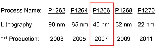
On track for first production by the end of 2007 with the Penryn family of processors (mobile, desktop and server), is Intel's 45nm manufacturing process. As with any move to smaller transistors, the 45nm node will make chips smaller and run faster. Intel is actually seeing good feature scaling with its 45nm process, quoting a ~2x improvement in transistor density. In other words, if you took a 100mm^2 65nm chip and built it on Intel's 45nm process, it would be roughly a 50mm^2 chip after the shrink. While logic and cache structures generally end up scaling very well with a process shrink, I/O structures (e.g. main memory interface circuits) don't which is why the improvement in transistor density is roughly and not exactly 2x.
Of course, in the past Intel has usually coupled new process technology with more features so you shouldn't expect to see 45nm Penryn chips as simply smaller Core 2 Duos. We will look at Penryn's die in a moment, but a larger cache, SSE4 and other unannounced microarchitectural enhancements can be expected.
The story of Intel's 45nm process doesn't end with details on its feature scaling however. Intel has made some fairly significant changes to the transistors themselves that make them more efficient than normal.
More Efficient Transistors
The basic function of a transistor as found in modern day microprocessors is to act as a switch with two states: on and off. When the transistor is on, current is allowed to flow from one terminal to the other (source to drain), and when it is off current shouldn't flow. Making enough current flow when it should and minimizing the amount that flows when it shouldn't is one of the major hurdles to making smaller transistors that run cooler/faster.
Below we have a typical CMOS transistor diagramed and labeled:
![]()
The voltage present at the Gate and the Source will determine whether or not current will flow in the transistor. Intel's 45nm process makes significant changes to two of the components in this transistor diagram: the gate electrode and the gate dielectric.
You can probably guess that as transistors get smaller, all of the parts of the transistor get smaller as well. The problem is that when some of these features get too small, they start behaving inappropriately. Case in point is the gate dielectric; with Intel's 90nm and 65nm processes, the gate dielectric was shrunk to a thickness of 1.2nm - the equivalent of about 5 atoms. The benefit of a very thin gate dielectric is that it increases the gate field effect, which increases drive current and reduces Source-drain leakage current. However, with such a thin gate dielectric electrons can tunnel directly through the layer and show up as leakage current - in other words, current would flow when it was not supposed to, translating into power wasted. On an individual transistor scale it's not such a big deal, but when you keep in mind that Penryn will have around 410 million of these transistors (820 million for quad-core) the leakage current/power draw does add up.
At 1.2nm, the gate oxide/gate dielectric in Intel's 90nm and 65nm transistors was as thin as Intel could make it without losing a great deal of power due to gate oxide leakage current. In order to make the move to 45nm Intel had to do something to thin the gate oxide without drastically increasing gate oxide leakage current.
Intel solved the gate oxide leakage problem by replacing the SiO2 gate dielectric with a material that has a higher k-value, in this case a Hafnium based material. A high-k dielectric here actually increases drive current at the same thickness as the previous SiO2 dielectric, while reducing gate leakage as well. Intel isn't disclosing how thick the Hafnium gate dielectric layer is in its 45nm transistors, but we do know that it is thicker than the 1.2nm SiO2 gate dielectric used in previous 90nm and 65nm transistors.
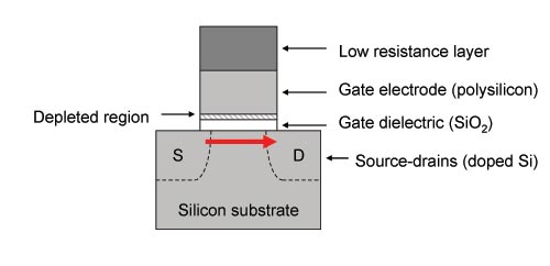
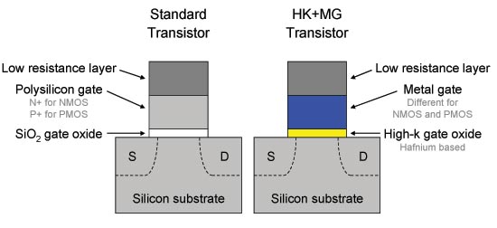
The second problem Intel is addressing with its 45nm transistors is a fundamental issue with the polysilicon gate electrode. The role of the gate electrode is important as it is what enables current to be driven through the transistor and as such it plays a role in how much current can be delivered. The polysilicon material that the gate electrode is made of has a tendency to form a region of depleted conducting carriers at the bottom of the gate, which reduces the drive strength of the transistor (less current flows when it needs to).
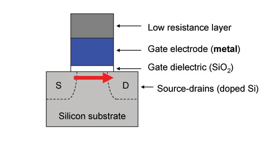
Intel's new 45nm transistors solve this problem by replacing the polysilicon gate electrode with a metal gate electrode, which completely eliminates the depleted region thus increasing the drive current.
Intel has been researching this High-k + Metal Gate (HK+MG) combination in transistors for a handful of years now, with hundreds of material options for metal gate electrodes and high-k dielectrics. The actual combination of high-k and metal gate material isn't being disclosed at this time, most likely to protect Intel's research and maintain the manufacturing advantage as long as possible. Intel expects that no other company will have HK+MG transistors until they reach 32nm or later.
The tangible advantages of these changes in materials in combination with the smaller 45nm process are quite large. According to Intel, the move from 65nm to 45nm yields a 30% reduction in transistor switching power because of the simple fact that smaller transistors have less parasitic capacitance and require less power to switch on and off.
Because of the combination of a high-k dielectric and the metal gate electrode, Intel is quoting a greater than 20% improvement in switching speed compared to its 65nm transistors. At the same speed as its 65nm transistors, there's a greater than 5x reduction in source-drain leakage power and a greater than 10x reduction in gate oxide leakage power; the latter is due entirely to the use of a high-k dielectric in the transistor. The end results of all of this are more power efficient processors, the first of which we should see by the end of this year.
Conroe has a Son: Introducing Penryn
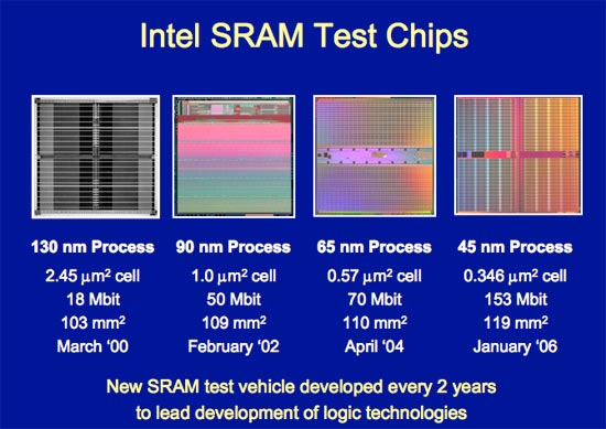
Intel announced the first working high-k + metal gate transistors back in 2003. By 2006 it had built an SRAM test vehicle (a wafer full of nothing but cache and some control/test logic) using the new transistors to work out most of the kinks in the manufacturing process.
Today, Intel is announcing that its first full CPU built using the new 45nm high-k + metal gate transistors is not only up and running, but it has also booted four OSes. The very first packaged Penryn silicon from the very first wafer booted Windows Vista, Mac OS X, Windows XP and Linux on the first try.
The picture below is of Intel's validation team after they successfully booted Penryn on the above OSes. The chips arrived in the lab at around 1AM and by 3AM they were up and running. If you're concerned, that's sparkling cider in those glasses and not champagne; alcohol is not allowed on Intel's campus, as it tends not to bring out the best in CPU designs, although it does make benchmark scores look infinitely higher.

It's a fairly big accomplishment to have first silicon working this well, but Intel has had a number of successful first spins in recent history. Generally by the time you're making your first CPUs, you've got the majority of the manufacturing defects worked out thanks to your SRAM test vehicle, so any problems with the first silicon are usually due to errors in the design or in the masks.
Intel also proudly sent us a shot of the 45nm Penryn die:
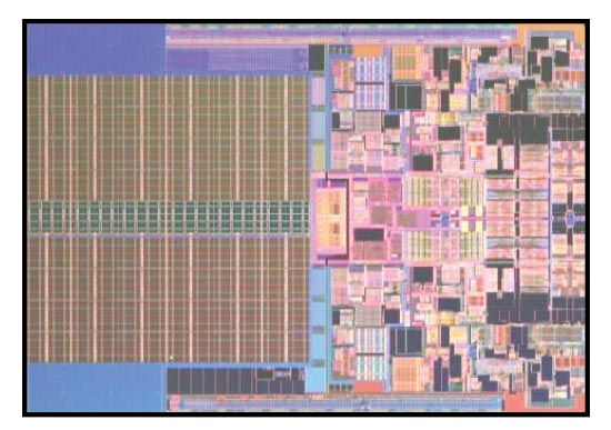
This version of Penryn is dual-core, and the first quad-core Penryn chips will simply be two of these on a single package, although later on we may see a single-die solution. At 410 million transistors, we expect a dual-core Penryn to have a 6MB shared L2 cache (up from 4MB in Conroe). The logic part of the Penryn core will be mostly evolutionary from Conroe, but do expect additional functionality and performance from more than just a larger cache.
If we assume that 288M transistors (6T SRAM) will be used by the 6MB cache, that leaves 122M transistors for L1 cache and the rest of the core. Applying the same calculation to Conroe gives us 99M transistors left over, meaning that there are roughly 23% more core-logic, control and L1 transistors being used in Penryn than in Conroe.
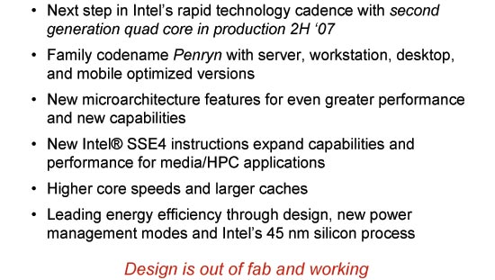
What that additional functionality will be is up in the air at this point, but you can expect SSE4 support to occupy a chunk of those transistors. At 45nm Intel should also be able to ramp up clock speed, so expect to see Penryn debut at over 3GHz easily. Given how overclockable Conroe turned out to be, we wouldn't be too surprised to see Penryn scale very well.
And the last bit of Penryn information Intel is letting out today is that it demonstrated Penryn up and running actual applications at a press briefing in Santa Clara on January 25th. There were five Penryn systems configured and clocked as follows:
1) 45nm dual core mobile processor in a notebook with Microsoft Vista running Microsoft Office 2003 applications.
2) 45nm dual-core desktop processor running high definition video content (1080P) under Microsoft Vista. 2.13 GHz
3) 45nm quad-core desktop processor running Ubisoft Rainbow Six Las Vegas game under Microsoft Vista. 1.86 GHz
4) Two 45nm dual-core processors running Glaze Workstation application under Microsoft Windows 2000 Advanced Server. 2.13 GHz
5) Two 45nm quad-core processors encoding a video in Adobe Premier under Microsoft Vista. 2.13 GHz
All of the systems were air-cooled using normal heatsink/fan units. Unfortunately Intel wouldn't share any benchmarks or more details of the systems other than what software they were running.
At this stage in the game it's normal to see clock speeds much lower than final shipping silicon, but this is the first time that Intel has been so forthcoming with clock speed data this far before launch. What we're seeing is a far more proud and confident Intel, and honestly it has every reason to be given the recent successes of Core 2 and promise of Penryn.
Yields and Manufacturing
Intel is sharing its usual vague data on yields at 45nm, but at least this time we get pretty good reference points to previous manufacturing processes. The graph below shows defect density as a function of time; you should keep in mind that processors generally don't start shipping until the very bottom of these curves in order to make the economics work for the CPU maker.
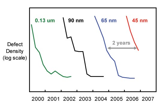
As you can see, 45nm is on a curve very similar to that of Intel's 65nm process, which means that things are on track for a smooth introduction later this year barring any unforeseen issues.
Intel attributed the rough patches in the 90nm trend to difficulty associated with building the first strained silicon transistors and using low-k interconnect dielectrics. By comparison, 65nm and 45nm appear to be much smoother sailing.
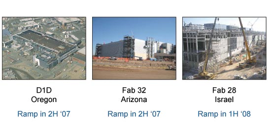
By the end of this year the first 45nm chips will be built at two 300mm Intel fabs: D1D in Oregon and Fab 32 in Arizona. Starting in the first half of 2008, Fab 28 in Israel will begin producing 45nm parts and should reach full capacity by the end of the year.
Final Words
It's very rare to get this much information out of Intel this far in advance of an actual product launch, but we're not complaining. By the middle of this year, AMD will launch its next-generation microarchitecture that will hopefully be a far better competitor to Intel's Core 2 processors. But before the year is out, Intel will respond yet again with its Penryn family of processors. We're unsure exactly what segments will be targeted first with Penryn, but by sometime in 2008 you should be able to get Penryn based notebooks, desktops and servers.
The inevitable comparison to AMD's progress on 45nm has to be made, but at this point we don't know too much. AMD revealed its 45nm SRAM test vehicle about three months after Intel did last year, with a slightly larger SRAM cell size (0.370 um^2 vs. 0.346 um^2 for Intel). The main focus for AMD at this point is the transition to 65nm; we're finally starting to see Brisbane cores available for purchase, but the highest clock speed offerings are still built on 90nm.
For Intel, we see continued strengthening and a roadmap that has a lot of promise. Penryn should be out sometime in the second half of this year, followed by a brand new architecture under the codename Nehalem. Nehalem will also be the first time we get to see an architecture change post-Core 2 under Intel's new tick-tock model of introducing new architectures every two years. It's quite possible that in the next two years Intel will have made the CPU industry far more exciting than it has been in the previous five (Core 2 launch withstanding).


