Original Link: https://www.anandtech.com/show/1647
Understanding the Cell Microprocessor
by Anand Lal Shimpi on March 17, 2005 12:05 AM EST- Posted in
- CPUs
Three very interesting things happened over the past couple of weeks here at AnandTech:
- Intel’s Spring IDF 2005 turned out to be a multi-core CPU festival, with Intel being even more open than ever before about future plans for their multi-core microprocessor architectures. Intel has over 10 multi-core CPU designs in the works, and they made that very clear at IDF.
- At GDC 2005, AGEIA announced that they had developed a Physics Processing Unit (PPU) that could be used to enable extremely realistic physics and artificial intelligence models.
- Johan De Gelas went one step further in his quest for more processing power earlier this week to find that there’s quite a lot of potential for multi-core CPUs in the gaming market, at the expense of increasing development times.
Cell, at a high level, isn’t too difficult to understand; it’s how the designers got there that is most intriguing. It’s the design decisions and building blocks of Cell that we’ll focus on here in this article, with an end goal of understanding why Cell was designed the way it was.
A joint venture between IBM, Sony and Toshiba, the Cell microprocessor is the heart and soul of Sony’s upcoming Playstation 3. However, this time around, Sony and Toshiba are planning to use Cell (or parts of it) in everything from consumer electronics to servers and workstations. If you don’t already have the impression, publicly, Cell has been given some very high aspirations as a microprocessor, especially a non-x86 microprocessor.
Usage Patterns
Before getting into the architecture of Cell, let’s talk a bit about the types of workloads for which Cell and other microprocessors are currently being built.In the past, office application performance was a driving factor behind microprocessor development. Before multitasking and before email, there was single application performance and for the most part, we were talking about office applications, word processors, spreadsheets, etc. Thus, most microprocessors were designed toward incredible single application, single task performance.
As microprocessors became more powerful, the software followed - multitasking environments were born. The vast majority of computer users, however, were still focused on single application usage, so microprocessor development continued to focus on single-threaded performance (single application, single task performance).
Over the years, the single-threaded performance demands grew. Microsoft Word was no longer the defining application, but things like games, media processing and dynamic content creation became the applications that ate up the most CPU cycles. This is where we are today with workloads being a mix of office, 3D games, 3D content creation and media encoding/decoding/transcoding that consume our CPU cycles. But in order to understand the creation of a new architecture like Cell, you have to understand where these workloads are headed. Just as the types of applications demanding performance today are much different than those run 10 years ago, the same will apply to applications in the next decade. And given that a new microprocessor architecture takes about 5 years to develop, it is feasible to introduce a new architecture geared towards these new usage models now.
Intel spoke a lot about future usage models at their most recent IDF, things like real time voice recognition (and even translation), unstructured search (e.g. Google image search), even better physics and AI models in games, more feature-rich user interfaces (e.g. hand gesture recognition), etc. These are the usage models of the future, and as such, they have a different set of demands on microprocessors and their associated architectures.
The type of performance required to enable these types of usage models is significantly higher than what we have available to us today. Conventionally, performance increases from one microprocessor generation to the next by optimizing single thread performance. There are a number of ways of improving single thread performance, either by driving up the clock speed or by increasing the instructions executed per clock (IPC). Taking it one step further, the more parallelism you can extract from a single thread, the better your performance will be - this type of parallelism is known as instruction level parallelism (ILP) as it involves executing as many instructions out of a thread at the same time.
The problem with improving performance through increasing ILP is that from one generation to the next, you’re only talking about a 10% - 20% increase in performance. Yet, the usage models that we’re talking about for the future require significantly more than the type of gains that we’ve been getting in the past. With power limitations preventing clock speeds from scaling too high, it’s clear that there needs to be another way of improving performance.
The major players in the microprocessor industry have all pretty much agreed that the only way to get the type of performance gains that are necessary is by moving towards multi-core architectures. Through a combination of multithreaded applications and multi-core processors, you can get the types of performance increases that should allow for these types of applications to be developed. Instead of focusing on extracting ILP to improve performance, these multi-core processors extract parallelism on a thread level to improve performance (thread level parallelism - TLP).
It’s not as straightforward as that, however. There are a handful of decisions that need to be made. How powerful do you make each core in your multi-core microprocessor? Do you have a small array of powerful processors or a larger array of simpler processors? How do they communicate with one another? How do you deal with feeding a multi-core processor with enough memory bandwidth?
The Cell implementation is just one solution to the problem...
High Level Overview of Cell
Cell is just as much of a multi-core processor as the upcoming multi-core CPUs from AMD and Intel, the only difference being that Cell's architecture doesn't have an entirely homogeneous set of cores.Cell's Execution Cores
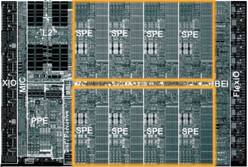
The Cell architecture debuted in a configuration of 9 independent cores: one PowerPC Processing Element (PPE) and eight Synergistic Processing Elements (SPEs). The PPE and SPEs are obviously different, but all eight SPEs are identical to one another.The PPE is IBM's major contribution to the Cell project; it also appears to be very similar to the core being used in the next Xbox console.
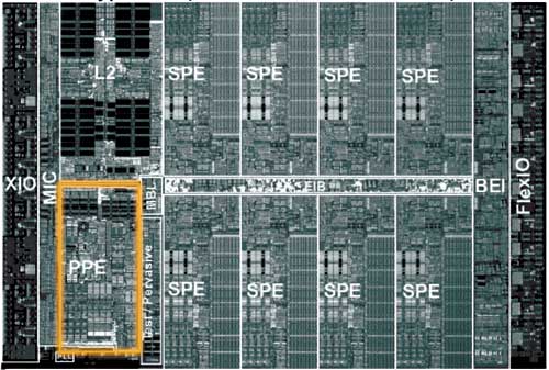
The PPE features a 64KB L1 cache and a 512KB L2 cache and features SMT, similar to Intel's Hyper Threading. The PPE features a strictly in-order core, which the desktop x86 market hasn't seen since the death of the original Pentium (the Pentium Pro brought out-of-order execution to the x86 market), so the move for an in-order core is an interesting one. The PPE is also only a 2-issue core, meaning that, at best, it can execute two instructions simultaneously. For comparison, the Athlon 64 is a 3-issue core, so immediately, you get the sense that the PPE is a much simpler core than anything that we have on the desktop. IBM's VMX instruction set (aka Altivec) is also supported by the PPE. Much like the rest of the Cell processor, the PPE is designed to run at very high clock speeds.
There's not much that's impressive about the PPE, other than it's a small, fast, efficient core. Put up against a Pentium 4 or an Athlon 64, the PPE would lose undoubtedly, but the PPE's architecture is one answer to a shift in the performance paradigm. Performance in business/office applications requires a very powerful, very fast general purpose microprocessor, but performance in a game console, for example, does not. The original Xbox used a modified Intel Celeron processor running at 733MHz, while the fastest desktops had 2.0GHz Pentium 4s and 1.60GHz Athlon XPs. Given that the first implementation of Cell is supposed to be Sony's Playstation 3, the simplicity of the PPE is not surprising. Should Cell ever make its way into a PC, the PPE would definitely have to be beefed up, or at least paired with multiple other PPEs.
The majority of the Cell's die is composed of the eight Synergistic Processing Elements (SPEs). If you consider the PPE to be a general purpose microprocessor, think of the SPEs as general purpose processors with a slightly more specific focus.
The SPEs have no branch predictor, meaning that they rely solely on software branch prediction. There are ways that the compiler can avoid branches, and the SPE architecture lends itself very well to things like loop unrolling. Any elementary programmer is familiar with a loop, where one or more lines of code is repeated until a certain condition is met. The checking of that condition (e.g. i < 100) often results in a branch, so one way of removing that branch is simply to unroll the loop. If you have a statement in a loop that is supposed to execute 100 times, you could either keep it in the loop and execute it that way, or you could remove the loop and simply copy the statement 100 times. The end result is the same - the only difference is that in one case, you have a branch condition while the other case results in more lines of code to execute.
The problem with loop unrolling is that you need a large number of registers to unroll some loops, which is one reason that each SPE has 128 registers. Originally, the SPEs were supposed to use the VMX (Altivec) ISA, but because of a need for more than 32 architectural registers, the SPEs implemented a new ISA with support for 128 registers.
Each SPE is only capable of issuing two instructions per clock, meaning that at best, each SPE can execute two instructions at the same time. The issue width of a microprocessor can determine a big part of how large the microprocessor will be; for example, the Itanium 2 is a 6-issue core, so being a 2-issue core makes each SPE significantly smaller than most general purpose microprocessors.
In the end, what we see with the SPEs is that they sacrifice some of the normal tricks to improve ILP in favor of being able to cram more SPEs onto a single die, effectively sacrificing some ILP for greater TLP. Given the direction that the industry is headed, a move to a very TLP centric design makes a lot of sense, but at the same time, it will be quite dependent on developers adhering to very specific development models.
Clearly, the architects of Cell saw the SPEs as being used to run a highly parallelizable workload, and as Derek Wilson mentioned in his article about AGEIA's PhysX PPU:
"One of the properties of graphics that made the feature a good fit for a specialized processor inside a PC is the fact that the task is infinitely parallelizable. Hundreds of thousands, and even millions of pixels, need to be processed every frame. The more detailed a rendering needs to be, the more parallel the task becomes. The same is true with physics. As with the visual world, the physical world is continuous rather than discrete. The more processing power we have, the more things we can simulate at once, and the more realistically we can approximate the real world."
With NVIDIA supplying some form of a GPU for Playstation 3, Cell's array of SPEs have one definite purpose in a gaming console - physics and AI processing. Many have argued that the array of SPEs seems capable of taking over the pixel processing workload of a GPU, but for a high performance console, that's not much of an option. The SPE array could offer better CPU-based 3D rendering, but it would be a tough sell (no pun intended) for this array of SPEs to be the end of dedicated GPU hardware.
Cell’s On-Die Memory Controller
For years, we’ve known that Rambus’ memory and interface technology is well ahead of the competition. The problem is that it has never been implemented well on a PC before. The Rambus brand received a fairly negative connotation during the early days of RDRAM on the PC, and things worsened even more for the company’s brand with the Rambus vs. the DDR world lawsuits.Rambus has had success in a lot of consumer electronics devices, such as HDTVs and the Playstation 2, so when Cell was announced to make heavy use of Rambus technologies, it wasn’t too surprising. As we’ve reported before, Rambus technology is used in about 90% of the signaling pins on Cell. The remaining 10% are mostly test pins, so basically, Rambus handles all data going in and out of the Cell processor. They do so in two ways:
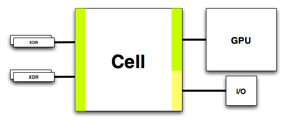
First off, Cell includes an on-die dual channel XDR memory controller, each channel being 36-bits wide (32-bits with ECC). Cell’s XDR memory bus runs at 400MHz, but XDR memory transfers data at 8 times the memory bus clock - meaning that you get 3.2GHz data signaling rates. The end result is GPU-like memory bandwidth of 25.6GB/s. As we’ve mentioned in our coverage of this year’s Spring IDF, memory bandwidth requirements increase tremendously as you increase the number of processor cores - with 9 total in Cell, XDR is the perfect fit. Note that the GeForce 6800GT offers 32GB/s of memory bandwidth just to its GPU, so it would not be too surprising to see the Playstation 3’s GPU paired up with its own local memory as well as being able to share system memory and bandwidth.
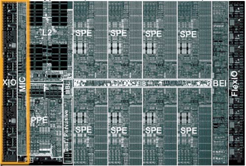
The block labeled MIC is the XDR memory controller, and the XIO block is the physical layer - all of the input receivers and output drivers are in the XIO block. Data pipelines are also present in the XIO block.
Cell’s On-Die FlexIO Interface
The other important I/O aspect of Cell is also controlled by Rambus - the FlexIO interface. Cell features two configurable FlexIO interfaces, each being 48-bits wide with 6.4GHz data signaling rates.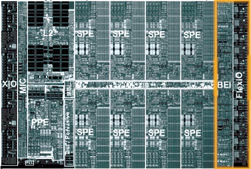
The BEI block is effectively the North Bridge interface, while the FlexIO block is the physical FlexIO layer.
One potential implementation of Cell’s configurable FlexIO interface.
In Playstation 3, you can pretty much expect a good hunk of this bandwidth to be between NVIDIA’s GPU and the Cell processor, but it also can be used for some pretty heavy I/O interfaces.
One of the major requirements in any high performance game console is bandwidth, and thanks to Rambus, Cell has plenty of it.
Cell’s In-Order Architecture
We have mentioned that both the PPE and SPEs are in-order cores, but in order to understand the impact of an in-order core on performance, there’s a bit of background knowledge that we have to go over first.Dependencies, Instruction Ordering and Parallelism
What are Dependencies?In many of our past CPU articles, we’ve brought up this idea of dependencies as seen by the CPU. At the very basic level, a CPU is fed a stream of instructions that are generally of the form:
OP destination, source1, source2, ... , source n
The instruction format will vary from one CPU ISA to the next, but the general idea is that the CPU is sent an operation (OP), a destination to store the result of the operation, and one or more sources on which to get data to perform the operation. Depending on the architecture, the destination and sources can be memory locations or registers. For the sake of simplicity, let’s just assume that for now, all destinations and sources are registers.
Let’s take a look at an example with some data filled in:
ADD R10, R1, R2
The above line of assembly would be sent to the CPU, telling it to add the values stored in R1 (Register #1) and R2 and store the result in R10. Simple enough. Now, let’s give the CPU another operation to crunch on:
MUL R11, R10, R3
This time, we’re multiplying the values stored in R10 and R3, and storing the result in R11. As a single line of assembly, the above code is easily executed, but when placed directly after our first example, we’ve created a bit of a problem:
- ADD R10, R1, R2
- MUL R11, R10, R3
- ADD R9, R11, R4
The problem with a dependency is that it limits what can be executed in parallel. Take the Athlon 64, for example. It has three integer execution units, all of which are equally capable of executing the code (in a slightly revised, x86 assembly format, of course) that we used above. In theory, the Athlon 64 could execute three lines integer operations in parallel at the same time - assuming that no dependencies existed between the operations. In executing the above code, two of the Athlon 64’s integer execution units would go idle until the first line of code was executed.
Dependencies, such as the simple one that we talked about above, hinder the ability of modern day microprocessors to function to the best of their abilities. It’s like having three hands, but only being able to clean your room by picking up one item at a time; frustratingly inefficient.
Ordering Instructions around Dependencies
Luckily, there are solutions to the problem of dependencies in code; one tackles the problem in hardware, the other tackles the problem in software.The software compiler is responsible for producing the assembly code that is sent to the CPU for execution. Thus, with an intimate knowledge of the inner workings of the CPU, the compiler can, generally speaking, produce code that minimizes data dependencies.
There are microprocessor architectures that are dependent entirely on the compiler to extract parallelism, on the instruction level, while avoiding dependencies as much as possible. These architectures are known as in-order microprocessors.
In-Order Architectures
As the name implies, an in-order microprocessor can only execute instructions in the order that they are sent to the CPU. At best, the CPU can execute multiple instructions in parallel, but it has no ability to reorder the instructions to suit its needs better.If you have a good enough compiler, then an in-order microprocessor should be just fine. There are a couple of key limitations, however:
1. Binaries Compiled for in-order architectures are very architecture specific
Although both the Athlon 64 and the Pentium 4 are fully able to run x86 code, they contain vastly different microarchitectures, with different execution units and very different things that they are “good” at. If both of the aforementioned chips depended entirely on the compiler to extract parallelism and maximize performance, one would most definitely suffer. You could always have two versions of every program, but that tends to get large and messy - especially from an update/patches standpoint. The compiler has to be intimately aware of the architecture that it’s compiling for, which works in cases like a game console where you don’t have multiple vendors providing differently architected CPUs with a common ISA, yet not so well when you look at something like the desktop x86 market.
2. Unpredictable memory latencies
Cache is a good thing, most of the time. Cache on a microprocessor does its best to keep frequently used data at hand, so it can be made available to the CPU at very low latencies. The problem is that cache adds a level of unpredictability to how long it will take to get data from memory. A cache hit could mean that your data will be ready in 10 - 20 cycles. A cache miss could mean that it’ll be hundreds of cycles. With an in-order microprocessor, you can’t reorder instructions based on data availability, so if data isn’t available in cache and the CPU has to wait longer to pull it from main memory, the entire CPU has to sit and wait until that data is brought in from main memory. Even if other instructions could be executed, an in-order microprocessor has no logic to effectively handle the on-the-fly reordering of instructions to get around unpredictable memory latencies.
If you can find a way around the limitations of an in-order architecture, there are some very tangible benefits:
1. A much simplified microprocessor
Out-of-Order microprocessors have a significant amount of complexity added to them in order to deal with on-the-fly reordering of instructions. We will talk about them in greater detail in the next section. By moving this complexity to the software/compiler side, you greatly reduce the complexity of your microprocessor and save your transistor budget for other things that can yield better performance benefits. Less complexity also means less power consumed and heat dissipated.
2. Shorter pipeline
In order to deal with the reordering of instructions, generally speaking, a number of pipeline stages have to be added to the architecture, resulting in higher power consumption and demands for a more accurate branch predictor (thanks to an even higher branch prediction penalty). While the impact on pipeline depth isn’t as big of a deal for longer pipelined designs, for shorter designs, the increase can be 40% or more.
Historically, the idea of a simple in-order core has been one that’s been abandoned in favor of the obvious alternative: an out-of-order architecture.
Out-of-Order Architectures
In contrast to in-order architectures, there are out-of-order architectures. Out-of-order architectures still decode instructions in the original order of the program, and still retire the instructions in order, but the actual issue/execution of the instructions can be done out of order.Let's talk a bit about what all of this means. A CPU is useless if it changes the intent of the code fed to it. Frankly speaking, if you double-click on a file, your CPU would be rather useless if it executed a bunch of format commands instead. Although that's an extreme example, in order to ensure that things like that don't happen, a CPU must adhere to two rules:
- Instructions must be decoded (i.e. interpreted by the CPU to find out what they are asking it to do) in the original order of the program, and
- Instructions must retire in the original order of the program (i.e. the result of each operation must be written to memory/disk in the same order as it was sent to the CPU).
- LD R10, R11
- ADD R5, R10, R10
- ADD R9, R9, #1
- ...
With an in-order microprocessor, if the data being loaded in line 1 is contained within cache, then that instruction will take around 1 - 30 clock cycles to complete (varying depending on the architecture and which level of cache it is in). Line 2 would have to simply wait those 1 - 30 cycles before executing and then after it executed, line 3 could have its turn. If the requested data isn't stored in cache (maybe it's the first time that we're asking for that value and we haven't asked for anything near it in memory), then we have a problem. All of the sudden, line 1 doesn't take around 1 - 30 cycles to complete; now, it's going to take 200+ clock cycles to complete. For line 2, that's not such a big deal, since it can't execute until line 1 completes anyway, but for line 3, it could just as easily execute during the time that the CPU is waiting to get that load from memory. Any independent instructions following line 3 are also at the mercy of the cache miss.
With an out-of-order microprocessor, however, the situation of a cache miss isn't nearly as dramatic. The code is still decoded in order, meaning that it comes across instructions 1, 2 and 3 in the same order as the in-order CPU, but this time, we have the ability to execute line 3 ahead of lines 1 and 2 instead of idly waiting for line 1 to complete. In the event of a cache miss, this gives the out-of-order microprocessor a pretty big performance advantage, as it isn't sitting there burning away clock cycles while nothing gets done. So, how does the out-of-order CPU work?
If someone told you a list of things to do in any order that you wanted, you'd simply take in the list and get to it. But if they told you to report back the things that you've completed in the order in which they were told to you, you'd have to grumble and write them down first before reorganizing them to fit your needs.
An out-of-order CPU works pretty much the same way, except instead of a to-do list, it has an instruction window. The instruction window functions similarly to a to-do list - it has all of the decoded instructions in their original order and is kept as a record to make sure that those instructions retire in the order that they were decoded.
Alongside the instruction window, an out-of-order CPU also has a scheduling window - it is in this "window" where all of the reordering of instructions takes place. The scheduling window contains logic to mark dependent and independent instructions and send all independent ones to execution units while waiting for dependent instructions to become ready for execution.
As previously dependent instructions (e.g. instructions waiting on data from main memory or instructions waiting for other instructions to complete) become independent, they are then able to be executed, once again, in any order.
Right off the bat, you can tell that the addition of an instruction window, a scheduling window and all of the associated logic to detect independent instructions, not to mention the logic to handle out-of-order execution but in order retirement, all makes for a more complex microprocessor. But there is one other significant problem with out-of-order microprocessors - the increase in performance and instruction level parallelism is greatly dependent upon the size of the instruction window.
The larger you make this window, the more parallelism that can be extracted simply because the CPU is looking at a wider set of instructions from which to select independent ones. At the same time, the larger you make the window, the lower your clock speed can be.
Despite the downsides, all modern day x86 microprocessors are out-of-order cores, as keeping a single core simple isn't the top priority given advances in manufacturing processes. The benefits of an out-of-order architecture are two-fold:
- Dynamic reordering of instructions lets the CPU hide memory latencies, allowing for even higher clock speeds. For every cache miss, a Pentium 4 3.6GHz has to wait around 230 clock cycles to get data from main memory, which is a lot of idle time in the eyes of the CPU. Being able to make use of that idle time by executing other independent instructions in the meantime is one way in which architectures like the Pentium 4 and Athlon 64 get away with running at such high multiples of their memory frequency.
- Incremental increase in instruction level parallelism - by reordering instructions on the fly, out-of-order architectures can improve ILP as best as possible in areas where the compiler fails to.
The first thing to remember is that you can get pretty solid performance from an in-order architecture. The Itanium is an in-order microprocessor, based on a premise similar to Cell by which the compiler should be able to extract the sort of parallelism that of an out-of-order core. Current generation Itanium cores run at half the speed of modern day x86 cores, yet the CPU is able to execute around 2x the instructions per clock as the fastest x86 CPUs. To quote Intel's Justin Rattner in reference to Itanium, "an appropriately designed instruction set should lend itself to an in-order architecture without any problems." So, it's quite possible that the same could apply to Cell...
Cell’s Approach - In Order with no Cache
Remember that the Cell’s architects designed the processor while evaluating the incremental performance each transistor they used resulted in (somewhat exaggerated, they didn’t count every last one of the 234 million transistors, but they evaluated each architectural decision very closely). In doing so, the idea of in-order vs. out-of-order must have raised a huge debate, given the increased complexity that an out-of-order core would add.With the major benefit of out-of-order being a decrease in susceptibility to memory latencies, the Cell architects proposed another option - what about an in-order core with controllable (read: predictable) memory latencies?
In-order microprocessors suffer because as soon as you introduce a cache into the equation, you no longer have control over memory latencies. Most of the time, a well-designed cache is going to give you low latency access to the data that you need. But look at the type of applications that Cell is targeted at (at least initially) - 3D rendering, games, physics, media encoding etc. - all applications that aren’t dependent on massive caches. Look at any one of Intel’s numerous cache increased CPUs and note that 3D rendering, gaming and encoding performance usually don’t benefit much beyond a certain amount of cache. For example, the Pentium 4 660 (3.60GHz - 2MB L2) offered a 13% increase in Business Winstone 2004 over the Pentium 4 560 (3.60GHz - 1MB L2), but less than a 2% average performance increase in 3D games. In 3dsmax, there was absolutely no performance gain due to the extra cache. A similar lack of performance improvement can be seen in our media encoding tests. The usage model of the Playstation 3 isn’t going to be running Microsoft Office; it’s going to be a lot of these “media rich” types of applications like 3D gaming and media encoding. For these types of applications, a large cache isn’t totally necessary - low latency memory access is necessary, and lots of memory bandwidth is important, but you can get both of those things without a cache. How? Cell shows you how.
Each SPE features 256KB of local memory, more specifically, not cache. The local memory doesn’t work on its own. If you want to put something in it, you need to send the SPE a store instruction. Cache works automatically; it uses hard-wired algorithms to make good guesses at what it should store. The SPE’s local memory is the size of a cache, but works just like a main memory. The other important thing is that the local memory is SRAM based, not DRAM based, so you get cache-like access times (6 cycles for the SPE) instead of main memory access times (e.g. 100s of cycles).
What’s the big deal then? With the absence of cache, but the presence of a very low latency memory, each SPE effectively has controllable, predictable memory latencies. This means that a smart developer, or smart compiler, could schedule instructions for each SPE extremely granularly. The compiler would know exactly when data would be ready from the local memory, and thus, could schedule instructions and work around memory latencies just as well as an out-of-order microprocessor, but without the additional hardware complexity. If the SPE needs data that’s stored in the main memory attached to the Cell, the latencies are just as predictable, since once again, there’s no cache to worry about mucking things up.
Making the SPEs in-order cores made a lot of sense for their tasks. However, the PPE being in-order is more for space/complexity constraints than anything else. While the SPEs handle more specified tasks, the PPE’s role in Cell is to handle all of the general purpose tasks that are not best executed on the array of SPEs. The problem with this approach is that in order to function as a relatively solid performing general purpose processor, it needs a cache - and we’ve already explained how cache can hurt in-order cores. If there’s a weak element of the Cell architecture it’s the PPE, but then again, Cell isn’t targeted at general purpose computing, despite what some may like to spin it as.
The downsides of an in-order PPE are minimized as much as possible by making the core only 2-issue, meaning that at best, it could execute two operations in parallel. So, execution potential lost to in-order inefficiencies are minimized in a sense that at least there aren’t a lot of transistors wasted on making the PPE an extremely wide chip. A good compiler should be able to make sure that both issue ports are populated as frequently as possible, despite the fact that the microprocessor is in-order. The PPE is also capable of working on two threads at a time, also designed to mask the inefficiencies of an in-order core for general purpose code.
Architecturally, if anything will keep Cell out of being used in a PC environment, it’s the PPE. A new Cell with a stronger PPE or an array of PPEs could change that, however.
Manufacturing, Die Size and Clock Speed
Intel's superiority in manufacturing is responsible for the majority of their technological advances in microprocessors over the past decade, and it's often argued that there isn't a company around that could come close to matching Intel's manufacturing abilities - with the exception of IBM.The Cell prototype boasts some pretty major manufacturing specs:
- 90nm SOI manufacturing process
- 221 mm2 die area
- 234M transistors
- > 4GHz observed clock speed
When it was first announced, the chip sounded massive, but its specifications compare extremely well to Intel's upcoming Pentium D processor; let's take a look at its vitals:
Intel Pentium D Processor
- 90nm strained silicon manufacturing process
- 206 mm2 die area
- 230M transistors
- 2.8GHz - 3.2GHz clock speed
With a slightly larger chip and a few million transistors more, Cell is supposed to be able to run at a minimum of 25% higher clock frequency than Intel's forthcoming Pentium D. We'll let that sit in for a moment...
Dynamic Logic
At first glance, a 90nm SOI Cell running at between 3 - 5GHz looks extremely impressive. After all, the fastest 90nm CPU IBM currently produces runs at 2.5GHz, not to mention that even Intel, the king of clock speed, can't mass produce anything faster than 3.8GHz on their 90nm process. But let's dig a little deeper.The Pentium 4 has two ALUs that run at twice its internal clock speed - so in the case of a Pentium 4 660, that means that two of the more frequently used execution units operate at 7.2GHz - on a 90nm process. So, it's possible to get circuits to run at higher clock speeds, even in the 3 - 5GHz range, on current 90nm processes - it just takes a little bit of creative logic design.
It's been confirmed that Cell is using some sort of dynamic logic as opposed to static CMOS in order to control transistor counts and improve operating frequencies. Intel uses a number of specialized logic techniques in their double-pumped ALUs to reach their 7GHz+ operating frequencies, and Intel has discussed techniques that are similar to the dynamic logic used in Cell.
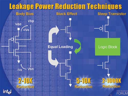
The diagram on the right of a "sleep transistor" should look very familiar by the end of this article
Transistors and You
Just about any AnandTech reader who has followed our CPU articles has heard us count transistors before, but understanding how transistors work is quite critical to understanding how IBM can talk about 3 - 5GHz clock speeds for Cell.We'll spare you the details about how transistors are made and the physics behind them in an attempt to keep this section as brief, but as informative, as possible. It's quite common to refer to a transistor as a "switch" much like a light switch, so how does a transistor function like a switch? Below, we have a representation of a p-type transistor:
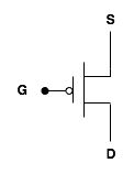
The input to the gate of the p-type transistor is what makes it function as a switch. If you apply the right voltage to the gate, thus making it a logical "1" or high, current doesn't flow in the transistor. If you don't apply any voltage to the gate, current can flow. Just like a light switch, flip it one way and the light turns on; flip it another and you're in the dark.
There's another type of transistor that we'll be talking about here: the n-type transistor:
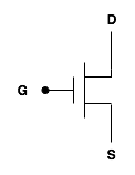
CMOS circuits work by using pairs of n- and p-type transistors (that's where the Complementary element of CMOS comes from). CMOS circuits are by far the most predominant in modern day microprocessors, but as you will soon see, that doesn't mean that they are without flaws.
Understanding Gates
The fundamental building blocks of any microprocessor are gates. Gates are collections of transistors that electrically mimic a particular logic function. For example, a 2-input AND gate will take two input signals and output a 1 only if the two inputs are both 1s. An XOR gate will output a 1 only if the two inputs are different. A NOR gate will output a 1 only if all inputs are 0s.Combinations of these gates are used to implement everything in a microprocessor, including functional units like adders, multipliers, etc.
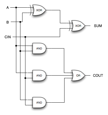
Here, we have a 1-bit carry adder implemented using logic gates. It will add any two 1-bit numbers and produce a result.
A very popular way of designing gate logic is using what is known as static CMOS. Static CMOS designs are relatively easy to implement and there are tons of libraries available for automated (e.g. computer driven) static CMOS design. There are a couple of problems with static CMOS design:
- Static CMOS circuits aren’t the fastest circuits possible, which is why they aren’t used in things like Intel’s double-pumped ALUs where high clock speeds are necessary.
- Static CMOS designs use quite a few transistors. For each m-input gate, you need 2 * m transistors (m PMOS and m NMOS transistors), which for high fan-in gates (gates with lots of inputs), it drives transistor counts up considerably. As is the case with any heavily SIMD architecture, high fan-in gates are commonplace.
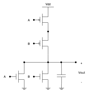
There’s another problem here - the NOR gate isn’t clocked. Normally, large collections of gates are assembled and put behind an element called a latch, which is clocked. One type of large collection would be all of the circuitry used for a pipeline stage. This isn’t really a problem for static CMOS gates, as it greatly simplifies the distribution of clocks to the chip (since you don’t have to route a clock signal to every gate, just every latch, and there are far more general gates than there are latches).
Designing and implementing static CMOS gates are extremely easy. Hardware Description Languages (HDLs), programming languages in which chips are “written” have widespread static CMOS libraries, meaning that a chip designer can focus on writing code to crank out a chip without having to hand design its circuits. But as success is usually proportional to difficulty, static CMOS designs aren’t the fastest things in the world. Things like Intel’s 7.2GHz ALUs aren’t designed using static CMOS logic, neither is Cell.
Cell’s Dynamic Logic
Although it’s beyond the scope of this article, one of the major problems with static CMOS circuits are the p-type transistors, and the fact that for every n-type transistor, you also must use a p-type transistor.There is an alternative known as dynamic or pseudo-NMOS logic, which gets around the problems of static CMOS while achieving the same functionality. Let’s take a look at that static CMOS NOR gate again:
Thus, the NOR gate outputs a 1 only if all inputs are 0, which is exactly how a NOR gate should function.
Now, let’s take a look at a pseudo-NMOS implementation of the same NOR gate:
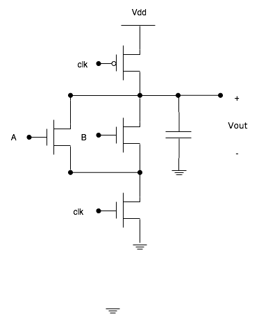
Cell’s implementation goes one step further. The p-type transistor at the top of the circuit and the n-type transistor at the bottom are clocked on non-overlapping phases, meaning that the two clocks aren’t high/low at the same time.
The way in which the gate here works is as follows: inputs are first applied to the logic in between the clock fed transistors. The top transistor’s gate is closed allowing the logic transistors to charge up. The gate is then opened and the lower transistor’s gate is closed to drain the logic transistors to ground. The charge that remains is the output of the circuit.
What’s important about this is that since power is only consumed during two non-overlapping phases, overall power consumption is lower than static CMOS. The downside is that clock signal routing becomes much more difficult.
The other benefit is lower transistor count. In the example of the 2-input NOR gate, our static CMOS design used 4 transistors, while our pseudo-NMOS implementation used 4 transistors as well. But for a 3-input NOR gate, the static CMOS implementation requires 6 transistors, while the pseudo-NMOS implementation requires 5. The reasoning is that for a CMOS circuit, you have 1 p-type transistor for every n-type, while in a pseudo-NMOS circuit you only have two additional transistors beyond the bare minimum required to implement the logic function. For a 100-input NOR gate (unrealistic, but a good example), a static CMOS implementation would require 200 transistors, while a pseudo-NMOS implementation would only require 102.
By making more efficient use of transistors and lowering power consumption, Cell’s pseudo-NMOS logic design enables higher clock frequencies. The added cost is in the manufacturing and design stages:
- As we mentioned before, clock routing becomes increasingly difficult with pseudo-NMOS designs similar to that used in Cell. The clock trees required for Cell are probably fairly complex, but given IBM’s expertise in the field, it’s not an insurmountable problem.
- Designing pseudo-NMOS logic isn’t easy, and there are no widely available libraries from which to pull circuit designs. Once again, given IBM’s size and expertise, this isn’t much of an issue, but it does act as a barrier for entry of smaller chip manufacturers.
- Manufacturing such high speed dynamic logic circuits often requires techniques like SOI, but once again, not a problem for IBM given that they have been working on SOI for quite some time now. There’s no surprise that Cell is manufactured on a 90nm SOI process.
Blueprint for a High Performance per Transistor CPU
Given that Cell was designed with a high performance per transistor metric in mind, its architecture does serve as somewhat of a blueprint for the technologies that result in the biggest performance gains, at the lowest transistor counts. Now that we’ve gone through a lot of the Cell architecture, let’s take a look back at what some of those architectural decisions are:1. On-die memory controller
We’ve seen this with the Athlon 64, but an on-die memory controller appears to be one of the best ways to improve overall performance, at minimal transistor expenditure. Furthermore, we also see the use of Rambus’ XDR memory instead of conventional DDR, as the memory of choice for Cell. High frequencies and high bandwidth are what Cell thrives on, and for that, there’s no substitute but Rambus’ technology.
2. SMT
On-die multithreading has also been proven to be a good way of extracting performance at minimal transistor impact. Introducing Hyper Threading to the Pentium 4’s core required a die increase of less than 5%, just to give you an idea of the scale of things. The performance benefits to SMT will obviously vary depending on the architecture of the CPU. In the case of the Pentium 4, performance gains ranged from 0 - 20%. In the case of the in-order PPE core of Cell, the performance gains could be even more. Needless to say, if implemented well, and if proper OS/software support is there, SMT is a feature that makes sense and doesn’t strain the transistor budget.
3. Simpler, in-order, narrow-issue core - but lots of them
This next design decision is more controversial than the first two, simply because it goes against the design strategies of most current generation desktop microprocessors that we’re familiar with. By making the PPE and SPEs 2-issue only, each individual core still remains a manageable size. Narrower cores obviously sacrifice the ability to extract ILP, but doing so allows you to cram more cores onto a single die - highlighting the ILP for TLP sacrifice that the Cell architects have made.
Getting rid of the additional logic and windows needed for an out-of-order core helps further reduce transistor count, but at the expense of making sure that you have a solid compiler and/or developers that are willing to deal with more of the architecture’s intricacies to achieve good performance.
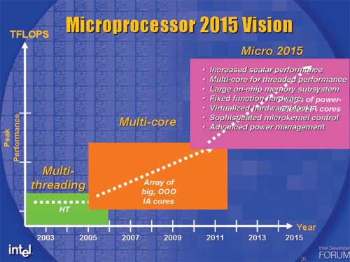
Looking at Intel’s roadmap for Platform 2015, the type of microprocessors that they’re talking about are eerily Cell-like - a handful of strong general purpose cores surrounded by smaller cores, some of which are more specialized hardware.
Final Words
Concluding anything about Cell requires a multifaceted look at the architecture and the platform as a whole.First from the perspective of the game industry, more specifically Playstation 3:
Cell’s architecture is similar to the next version of Microsoft’s Xbox and upcoming PC microprocessors in that it is heavily multithreaded. The next Xbox will execute between 3 and 6 threads simultaneously, while desktop PC microprocessors will execute between 2 - 4. The problem is that while Xbox 2/360/Next and the PC will be using multiple general purpose cores, Cell relies on more specialized hardware to achieve its peak performance. Cell’s SPEs being Altivec/VMX derived is a benefit, which should mean that the ISA is more familiar to developers working on any POWER based architecture, but the approach to development on Cell vs. development on the PC will literally be on opposite ends of the spectrum, with the new Xbox somewhere in between.
The problem here is that big game development houses often develop and optimize for the least common denominator when it comes to hardware, and offer ports with minor improvements to other platforms. Given Cell’s architecture, it hardly looks like a suitable “base” platform to develop for. We’d venture to say that a game developed for and ported from the PC or Xbox Next would be under-utilizing Cell’s performance potential unless significant code re-write time was spent.
Console-only development houses, especially those with close ties to Sony, may find themselves able to harness the power of Cell much more efficiently than developers who ascribe to the write-once, port-many process of cross-platform development. Given EA’s recent acquisition and licensing-spree, this is a very valid concern.
With Cell, Sony has effectively traded hardware complexity for programmer burden, but if anyone is willing to bear the burden of a complicated architecture, it is a game developer. The problem grows in complexity once you start factoring in porting to multiple platforms in a timely manner while still attempting to achieve maximum performance.
As a potential contender in the PC market, Cell has a very tall ladder to climb before even remotely appearing on the AMD/Intel radars. The biggest strength that the x86 market has is backwards compatibility, which is the main thing that has kept alternative ISAs out of the PC business. Regardless of how much hype is drummed up around Cell, the processor is not immune to the same laws of other contenders in the x86 market - a compatible ISA is a must. And as Intel’s Justin Rattner put it, “if there are good ideas in that architecture, PC architecture is very valuable and it will move to incorporate those ideas.”
Once again, what’s most intriguing is the similarity, at a high level, of Intel’s far future multi-core designs to Cell today. The main difference is that while Intel’s Cell-like designs will be built on 32nm or smaller processes, Cell is being introduced at 90nm - meaning that Intel is envisioning many more complex cores on a single die than Cell. Intel can make that kind of migration to a Cell-like design because their microprocessors already have a very large user base. IBM, Sony and Toshiba can’t however - Cell must achieve a very large user base initially in order to be competitive down the road. Unfortunately, seeing a future for Cell far outside of Playstation 3 and Sony/Toshiba CE devices is difficult at best.
The first thing you have to keep in mind is that Cell’s architecture is nothing revolutionary, it’s been done before. TI’s MVP 320C8X is a multi-processor DSP that sounds a lot like Cell: http://focus.ti.com/docs/military/catalog/general/general.jhtml?templateId=5603&path=templatedata/cm/milgeneral/data/dsp_320c80&familyId=44. So, while Cell is the best mass-market attempt at a design approach that has been tried before, it doesn’t have history on its side for success beyond a limited number of applications.
Regardless of what gaming platform you’re talking about, Cell’s ability to offer an array of cores to handle sophisticated physics and AI processing is the future. AGEIA’s announcement of the PhysX PPU (and the fact that it’s been given the “thumbs up” by Ubisoft and Epic Games) lends further credibility to Cell’s feasibility as a high performance gaming CPU.
The need for more realistic physics environments and AI in games is no illusion; the question is will Intel’s forthcoming dual and multi-core CPUs (with further optimized SIMD units) offer enough parallelism and performance for game developers, or will the PPU bring Cell-like architecture to the desktop PC well ahead of schedule? The answer to that question could very well shape the future of desktop PCs even more so than the advent of the GPU.


