Original Link: https://www.anandtech.com/show/1611
The Quest for More Processing Power, Part One: "Is the single core CPU doomed?"
by Johan De Gelas on February 8, 2005 4:00 PM EST- Posted in
- CPUs
Introduction
"What you have seen is a public demonstration of 4 GHz silicon straight off our manufacturing line. We have positive indications to be able to take Netburst to the 10 GHz space."
"While architectural enhancements are important, Intel intends to continue its lead in raw speed. Otellini demonstrated a new high-frequency mark for processors, running a Pentium 4 processor at 4.7 GHz."
The first assertion was made at IDF Spring 2002, and the second press release was broadcasted after Fall IDF 2002. Fast forward to the beginning of 2004, and we read in the Prescott presentation: "2005-2010: the era of thread level parallelism and multi-core CPU technology. " What happened to "the 10 GHz space"?
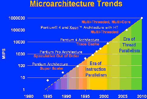
Fig 1. "2005-2010: the era of thread level parallelism and multi-core CPU technology ".
The presentation of the new 6xx Prescott even states that Intel is now committed to " Adding value beyond GHz". This sounds like Intel is not interested in clock speeds anymore, let alone 10 GHz CPUs.
Already, the hype is spreading: Dual core CPUs offer a much smoother computing experience; processing power will increase quickly from about 5 Gigaflops to 50 gigaflops and so on. It is almost like higher clock speeds and extracting more ILP (Instruction Level parallelism), which has been researched for decades now, are not important anymore.
At the same time, we are hearing that "Netburst is dead, Tejas is cancelled and AMD's next-generation K9 project is pushed back." Designs built for high clock speeds and IPC (Instructions per Clock) are no longer highly regarded as heroes, but black sheep. They are held responsible for all the sins of the CPU world: exploding power dissipation, diminishing performance increases and exorbitant investments in state of the art fabs to produce these high clock speed chips. A Prescott or Athlon 64 CPU in your system is out of fashion. If you want to be trendy, get a quad core P-m, also known as Whitefield [2], made in India.
To the point
I am exaggerating, of course. A good friend of mine, Chris Rijk, said: "PR departments having no 'middle gears': they either hype something to great lengths, or not at all." Trying to understand what is really going on is the purpose of this article. We are going to take a critical look at what the future CPU architectures have to offer. Is the traditional approach of increasing IPC and clock speed to get better performance doomed? Does multi-core technology overcome the hurdles that were too high for the single-core CPUs? Are multi-core CPUs the best solution for all markets? Will multi-core CPUs make a difference in the desktop and workstation market?
In this first instalment, we explore the problems that the current CPU architectures face. The intention is to evaluate whether the solution proposed by Intel and other manufactures is a long-term solution, one that really solves those problems. We will also investigate one CPU in particular, the Intel Prescott. So, basically there are 4 chapters in this article that will discuss:
- The problems that CPU architects face today: Wire Delay, Power and the Memory wall.
Chapter 1 - The brakes on CPU power - The reason why Intel and others propose dual core as a solution to these problems.
Chapter 2 - Why single core CPUs are no longer "cool" - Whether or not these problems can be solved without dual core.
Chapter 3 - Containing the epidemic problems - A case study of the Intel Prescott.
Chapter 4 - The Pentium 4 crash landing
Although Intel is undeniably the industry leader in the CPU market, this doesn't always mean that the solutions proposed are the right ones. For example, remember MMX, which was a technology that should have turned the (x86-based) PC into a multimedia monster. In hindsight, the critics were right. MMX was little more than a marketing stunt to make people upgrade.
The first implementation of hyperthreading on Intel's Foster Xeon (Willamette Xeon) was turned off by default by all OEMs. And hyperpipelined CPUs with 30+ stages turned out to be an impressive, but pretty bad idea.
In other words, not all hypes have turned out to be beneficial for the customer. Millions of customers are still waiting for the rich content on the Internet that is enabled by and runs so much faster on the Netburst architecture...
CHAPTER 1: The brakes on CPU power
CPU Performance increase hits the brakes.
The growth rate of CPU performance has been spectacular in the past decades. Two legends of computing history, John.L Hennessy and David A. Patterson, have quantified this performance growth to be about 58% per year.
A recent study by the University of göteborg [1] confirmed that the 58% number was true between 1985 and 1996. During the last 7.5 years (1996-2004), the Swedish professors proved that the performance growth has slowed down to an average of 41% per year. Even worse is the conclusion that "there are signs of a continuing decline".
When we focus on Intel's CPUs, the deterioration of CPU performance growth is almost spelling doom. In November 2002, Intel was well ahead of the competition with the introduction of a 3.06 GHz Pentium 4. Intel had doubled the clock speed of its latest x86 architecture within two years, which was quite an accomplishment.
Two and half years later, Intel's Pentium 4 is running at 3.8 GHz, which means that clock speed has increased by only 25%. Of course, we all know that performance does not scale linearly with clock speed. So, let us talk performance.
| CPU | SpecInt2000 | SpecFp2000 |
| Pentium 4 3800E | 1666 | 1839 |
| Pentium 4 3060 | 1167 | 1096 |
| Pentium 4 1500 | 560 | 634 |
From 2000 to 2002, performance increased by 108%. In the following 3 years, Intel's latest CPU only increased integer performance by 43%. The same does not hold true for SpecFP2000, as the 3.8 GHz Prescott CPU had improved performance by 68%, while the 3.06 GHz was about 73% faster than the first incarnation of the Netburst architecture.
However, SpecFP2000 remains a "special" benchmark, which exaggerates greatly the importance of memory bandwidth as very few other FPU applications behave the same way. The 800 MHz FSB of the 3.8 GHz is 50% faster than the bus to Intel's first Hyperthreaded CPU (3.06 GHz), while the FSB of the latter has only a 33% advantage over the older 1.5 GHz Pentium 4.
Intel's compilers have also improved vastly over the past years, which is positive. However, they have also become better in using special tricks (strip-mining optimizations, for example) to artificially improve the Spec score; tricks that are not usable by developers who need to get real applications to the market. Don't take my word for it, but make sure to read Tim Sweeney's comments in the next article.
These advantages are the main reasons why SpecFP doesn't tell us what most applications do: the pace of CPU performance growth has slowed down significantly, even in FP intensive workloads. Applications such as 3DSMax, Lightwave, Adobe Premiere, video encoding and others show, on average, that the Pentium 4 3.8 GHz is about 20-45% faster than the Pentium 4 3.06 GHz, while the latter is easily between 60% and 90% faster than our 1.5 GHz reference point.
Demystifying the slowdown
It is no mystery that the three main reasons why CPU progress is slowing down are:
- Total dissipated power
- Wire Delay
- "The memory wall"
However, simply stating that these three problems are the reason why it is getting very hard to design CPUs that perform better is an oversimplification. There are decent solutions for each of these problems, and the real reason why they have slowed down CPU progress is more subtle.
We are going to cover the memory wall in more detail later. Suffice it to say, it is well known that DRAM speeds up by about 10% per year, while CPUs run 40% to 60% faster each year.
Power problems
In order to understand power problems, you have to understand the following formula, which describes switching power:
Power ~ ½ CV ² Af
In other words, dissipated power is linear with the effective capacitance, activity and frequency. Power increases quadratically with the CPU's core voltage. Activity is the factor that is influenced by the software you run; the more intensive the software, the higher the amount of the time that the transistors are active.
With each major transition to a new process technology that has a reduction in transistor feature size of 2, the same die area becomes 4 times smaller. For example, Willamette (introduced with 180 nm technology) would have been more or less 4 times smaller using the 90 nm technology. That is simplified of course, but it shows that the die gets smaller and smaller. Now that should not be such a problem as Vdd (Vcore) can also be reduced, and as a result, you can reduce power by a factor of two or even more. Of course, as CPUs extract more ILP and have deeper pipelines, they become more complex and use more transistors. The result is that the power reductions of decreasing Vdd are negated by the increasing amount of transistors.
And there are limitations of the amount of power that you can dissipate through a shrinking die area. But switching power is not the worst problem, as it can be reduced by applying a few clever techniques.
One of them is clock gating, a power-saving technique implemented extensively in the Pentium 4. Clock gating logic will only activate the clocks in a Functional Unit Block (FUB) when it needs to work. Together with other power-saving techniques, switching or dynamic power is more or less under control; over time, it increases linearly, while the amount of transistors used is increasing exponentially.
When a CPU becomes a sieve
The real problem is leakage power, and the Intel power graph below illustrates this perfectly.
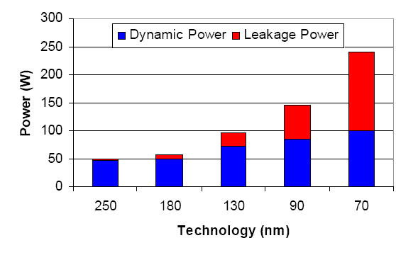
Fig 2. "Leakage power grows exponentially ".
As you can see, dynamic power - which does useful work - has increased relatively slowly despite the increase in CPU complexity. Leakage power, however, increases exponentially, and not linearly. It has grown quickly from a "minor nuisance" to a "circuit killing monster".
Leakage is comparable to a small hole in a waterhose of a firefighter. The more pressure (i.e. the higher the core voltage), the bigger the hole gets, and thus, the more water that leaks to the ground. The thinner the walls of the tube (i.e. smaller process technology), the quicker the holes become bigger, and the more water you lose, the harder the pumps must work to get the same amount of water to extinguish the fire. If the pumps overheat, you better throttle them down, or they will cease to work after a while.
Power Leakage happens as a part of the current, which is supposed to make our transistors switch leaks away in the substrate and finally in the ground. There are several leakage currents, but the two most important ones are the gate oxide tunnelling current and sub-threshold leakage.[3]
![]()
Fig 3. I3 is the Gate oxide tunnelling currents, I2 is the Sub-threshold leakage current
Gate oxide tunnelling (I3) currents get more important with smaller process technology as the gate oxide that is supposed to insulate the transistor becomes thinner and thinner. As a result, current that is going through the transistors leaks away - the gate oxide becomes a sieve instead of being the "wall of a tube".
Sub-threshold leakage (I2) transistor is the leakage current flowing through the transistor when it is supposed to be turned off. To understand this, we got to back to basic transistor technology.
Normally, a voltage threshold of x volts is needed to get current across the transistor, with x volts being the threshold. This way, the transistor is being used as a switch with a binary function: more or equal to threshold voltage = ON = 1, less than the threshold voltage = OFF.
The point that you have to remember is this: ideally, as long as the threshold voltage is not reached, no current should run through the transistor. However, as transistors and interconnects get smaller and smaller (smaller process technology), the insulation between drain and source gets worse and worse. As a result, a small leakage current gets through the transistor (I 2) even though the threshold voltage is not reached (the Transistor is off).
That subthreshold leakage has become a major problem, which has been made clear by Shekhar Borkar [5] (Intel Fellow, Director of Circuit Research). He illustrated this by the logarithmic graph below.
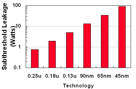
Fig 4. Subthreshold leakage - notice the logarithmic scale!
Subthreshold leakage was only a small problem at the time of Willamette - the leakage problem wasted a few watts at 180 nm. The graph is based on Moore's law: every two years, the number of transistors doubles. As you can see, without countermeasures, it wouldn't be interesting to use devices that make use of 45 nm technology. They would simply leak too much power, up to 100 Watts!
And subthreshold leakage is only part of the leakage problem. Together with gate oxide tunnelling, CPUs made of 65 nm technology would leak more power than what they need for making the transistors switch. It is comparable to a fuel tank that has so many holes, causing it to leak more gasoline to the ground than what the fuel pump can pump to the engine.
Let us check the third and last problem for high performance CPUs.
Wire delay
It is hard to imagine that the little wires - the metal interconnects - between transistors can be a limiting factor. About twenty years ago, transistor switching speeds were pretty low, and wire delays were completely ignored. However, as process technology became better, transistors were capable of switching much faster. Right now, the fastest transistors in the labs can attain 100 GHz (the record being around 300-500 GHz) and more. So, transistor switching speed still has a lot of headroom.
The tiny wires between the different transistors are still not the problem. Functional blocks are also wired to the TLBs (Translation Lookaside Buffer) and caches. The real problem is these global wires - they are a lot longer . If the RC delay is too high, the clock speed will have to be reduced to get a working CPU.
The speeds at which signals travel through the global wires (from logic blocks to the caches, for example) are quite a bit slower than what the maximum speed (speed of light) allows. The reason is the resistance (R, Ohm) and capacitive resistance (C) of the wire. As the whole CPU was made with smaller process technology, the wires also shrunk. You probably know from your lessons of physics that resistance increases as the cross section of the wire gets smaller and the length of the wire gets longer. So, if you shrink a wire, the effect of the shorter length is completely negated by the smaller thickness of the wire. You could make the wires thicker, but it wouldn't be easy and that would increase the capacitance of the wire. The result is that wire delay remains, more or less, the same (in nanoseconds).
However, gate switching speed improves a lot with smaller transistors (for example, 100%). So, while RC delay improves with a very small percentage (or nothing all), gates might switch up to 100% (simplified example) faster as process technology improves. The RC delay of the global wires becomes more a bottleneck that makes bumping up the clock speed hard. Modern Integrated Circuits (ICs), such as CPUs, must be partitioned, as a signal can travel for a time slightly less than the length of one clockpulse.
CHAPTER 2: Why single core CPUs are no longer "cool"
The end of the single core CPU?
Right now, the leakage problem is by far the most urgent problem. As profit margins are low and cost is, in most cases, the decisive factor for consumers, expensive cooling systems are not practical.
Past experience has shown that complex superscalar CPUs need about twice as many transistors to achieve +/- 40% better performance. The conclusion of many industry analysts and researchers is that the single-core CPU has no future. I quote Shekhar Borkar, Intel Fellow, Director:
"Multiprocessing, on the other hand, has potential to provide near linear performance improvement. Two smaller processors, instead of a large monolithic processor, can potentially provide 70-80% more performance, compare this to only 40% from the large monolithic processor."
Note the word "monolithic", a word with a rather pejorative meaning, which insinuates that the current single core CPUs are based on old technology. So, basically the single core CPU has no future as it improves performance only by 40%, while doubling complexity and thus leakage. This reasoning explains why all of sudden Intel marketing does not talk anymore about 10 GHz CPUs, but about the "era of thread parallelism".
It should be noticed though that the 40% better performance of the "monolithic CPU" is achieved across a wide variety of applications, without the need of time-consuming software optimizations. The promised 70% to 80% of the multithreaded CPU can only be easily achieved in a small range of applications, while the other applications will see exponential investments in development time to achieve the same performance increase.
Of course, we agree that multiprocessors have benefits. It is easier to turn off a complete CPU than to manage the energy consumption of the different parts of one big CPU.
And you can run a single-threaded application on CPU1, and turn the CPU2 off. When CPU1 gets almost hot, you let CPU2 continue to do the work. As a result, you reduce the average temperature of one CPU core. As leakage decreases with lower die temperatures, this technique can reduce overall leakage power. The objective of using a dual core CPU is then primarily to reduce power consumption in situations where there is only one CPU intensive application. This is probably the reason why Intel sees a great future for dual core CPUs in the mobile market, although the mobile market is probably the last market where we will be able to benefit from dual core power. The last thing that you want is twice as much power dissipation because the two cores get active. In our humble opinion, dual core will be only dual when it is not working on battery power.
Trendy
The second argument used by the people who are hyping the multithreaded CPU is "the whole industry is moving towards multi-core CPUs". Considering that the server is the only market where non x86 CPUs play an important role, it is not very surprising. For companies such as SUN and IBM, it is only natural to ignore single-threaded performance somewhat and to invest as much time as they can in designs that can work with as many threads as possible. The software that runs on these SUN and IBM machines, Massive OLTP databases and HPC applications, are multi-threaded by nature.
SUN's Niagra CPU can run 32 threads at once, but it will not be the kind of CPU that you would like in your desktop. Single threaded performance is most likely at the level of one of the early PIIIs. Sun's own demo [6] shows a Niagra to be more than 4 times slower in a single-threaded application than an unknown single-threaded CPU, which is, hopefully for SUN, one of the current top CPUs.
Delving deeper
So, while there are definite advantages to CPUs that exploit Thread Level Parallelism, if we want to understand what is really going on, we need to delve a little deeper. First, we look if leakage can really kill all progress of "monolithic" single core CPUs; secondly, we will study the prime example of a "classic" single core CPU that had crushed into a wall of leakage: the Intel Prescott.
CHAPTER 3: Containing the epidemic problems
Reducing leakage
Leakage is such a huge problem that it could, in theory, make any advance in process technology useless. Without countermeasures, a 45 nm Pentium 4 would consume 100 to 150 Watts on leakage alone, and up to burn 250 Watts in total. The small die would go up in smoke before the ROM program would have finished the POST sequence.
However, smart researchers have found ways to reduce leakage significantly. SOI – Silicon on Insulator - improves the insulation of the gate and thus reduces leakage currents. SOI has made process technology even more complex, making it harder for AMD to get high binsplits on the Opteron and Athlon 64. However, it is clear that the Athlon 64 has a lot less trouble with leakage power than the Prescott, despite the fact that the Athlon 64 has only 20% less transistors than the Intel Prescott (106 versus 125 million).
The most spectacular reduction of leakage will probably come from Intel's "high-k" materials, which will replace the current silicon dioxide gate dielectric. Thanks to this advancement and other small improvements, Intel expects to reduce gate leakage by over one hundredfold! This new technology will be used when Intel moves to 45nm technology.
Another promising technique is Gate Bias technology. By using special sleep transistors, leakage can be reduced by up to 90% while the dynamic power is also reduced with 50% and more.
Body Bias techniques make it possible to control the voltage of a transistor. The objective is to make transistors slow (low leakage) when they are not used, and fast when they are. Stacked transistors and many other technologies also allow for reduction in leakage.[4]
One could probably write a book on this, but the message should be clear: the leakage problem is not going to stop progress. SOI already reduces the problem significantly and high K materials will make sure that the whole leakage problem will remain to be a nuisance, but not a major concern until the industry moves to even smaller structures than 45 nm.
At the same time, strained silicon will reduce the amount of dynamic power needed. With strained silicon, electrons experience less resistance. As a result, CPUs can get up to 35 percent faster without consuming more. This is what should allow the Athlon 64 stepping "E0" to reach higher clock speeds without consuming more.
Reducing Wire Delay
Although wire delay has not been so much in spotlight as leakage power, it is an important hurdle that designers have to take when they target high clock speeds. The resistance of wires has been reduced by both AMD and Intel using copper instead of aluminium. Capacitance has been lowered by using lower-K materials separating wires.
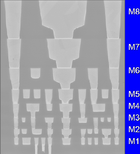
Fig 5. 8 Metal layers to reduce wire delay in Intel's 65 nm CPUs
Adding more metal layers is another strategy. More metal layers enable the wires connecting different parts of the CPU to be packed more densely. More densely means shorter wires. And shorter wires result in lower resistance, which, in turn, reduce the total RC Delay.
Fig 6. Repeaters on the Itanium Die
Of course, there are limits on what adding more metal layers, using SOI and lower-K materials can do to reduce RC delay. If some of the global wires are still too long, they are broken up into smaller parts, which are connected by repeaters. Repeaters can be used as much as you like, but they consume power of course.
Now that we have wire delay and leakage more or less out of control, let us try to find out what went exactly wrong with the Pentium 4 "Prescott". The answer is not as obvious as it seems.
CHAPTER 4: The Pentium 4 crash landing
The Prescott failure
The Pentium 4 "Prescott" is, despite its innovative architecture, a failure. Intel expected to scale this Pentium 4 architecture to 5 GHz, and derivatives of this architecture were supposed to come close to 10 GHz. Instead, the Prescott was only able to reach 3.8 GHz after numerous revisions. And even then, the 3.8 GHz is losing up to 115 Watt, and about 35-50% (depending on the source) is lost to leakage power.
The Prescott project failed, but that doesn't mean that the architecture itself was not any good. In fact, the philosophy behind the enhanced Netburst architecture is very innovative and even brilliant. To understand why we state this, let me quickly refresh your memory on the software side of things.
IPC unfriendly software
First, consider that the average code does not allow the CPU to process a lot of instructions in parallel. To give you an idea, we found out that video encoding achieves about 0.6-0.8 instructions per clock cycle (IPC) on modern CPUs. Secondly, note that almost 20% of the instructions are branches, and 50% of them are memory operations. In case of video encoding, you may have less than 10% branches, and about 60% memory operations. Most of the instructions that are not branches or memory operations are additions, or "ADD"s. Some of the memory operations need to make use of the same units that perform the ADD instructions.
You should also know that many algorithms contain calculations, which need the results of a previous one: a dependency. So, you cannot issue the second calculation until the first is done.
Most studies show that realistically, a sophisticated CPU would be able to reach an IPC of a little more than 2, about twice as much as CPUs today.
Up close and personal
Now, take look at the scheme of the Prescott architecture below. Let us see how Prescott solves all the problems mentioned above.

Fig 7. Prescott's architecture.
Click to enlarge.
First of all, you want to make sure that memory operations happen quickly. Therefore, the Prescott doubled the L1 (data only) and L2-cache. It has also two dedicated Address Generation Units, one for stores and one for loads.
Build for 4 GHz and more, accesses to the main RAM are going to be costly in terms of clock pulses (latency), considering that DDR-II 533 runs at a 266 MHz clock. So, Prescott tries to minimize the damage of waiting for cache misses by increasing the big store buffers of Northwood from 24 to 32, and doubling the load request buffers. So, Prescott can have a lot of cache misses simultaneously outstanding . An intelligent hardware prefetcher is another way to avoid slowdowns due to high memory latency.
To battle branch misprediction, the Prescott Branch predictor has been tuned and predicts 10% of the mispredicted branches by Northwood correctly. That results in up to 20% better performance! And of course, the trace cache makes sure that a mispredicted branch does not need to restart the decoding stages. As a result, the misprediction penalty is not 39 stages, but 31 stages. The 8 stages of decoding do not need to happen again because in most cases, the Trace cache has the decoded instruction.
Magic stone
ADDs need to happen quickly (they are very common) and dependent instructions should not wait long for the results that they need. Otherwise, the whole superscalar machine comes to a grinding halt and is not used efficiently. Intel's engineers killed those two birds with one magic stone: the double-pumped adder combined with a very smart Store-to-Load forward mechanism.
Consider this:
Instruction 1: C := D+D
Instruction 2: A := B+C
One instruction (2) needs the result (variable "C") of a previous one (1). In theory, the load of the variables of the second instruction cannot happen before the store of the first one has been written back. x86 ISA rules demand that stores happen in program order.
So, the second instruction won't have the necessary data before the first instruction has completed almost the entire pipeline (about 30 stages). That means that for 30 clock pulses, other independent instructions need to be found to keep the pipelines working. Modern CPUs try to offset this problem with Store-to-Load Forwarding. The forwarding mechanism kicks in as soon as the execution engine has calculated the result of the first instruction, and doesn't wait until all pipelines stages after the execution are done. The data is "forwarded" to the waiting instruction after a few clock cycles (as long as the calculation/execution takes), and way before the result has been written back to the L1 cache. Prescott's Store-to-Load Forwarding handles many store-forward situations, which are not forwarded by other "less intelligent" CPUs.
Cool & double pumped
If ADDs need to be executed fast, and store-to-forwards must happen very early in the pipeline, you need low latency ADD ALUs (Arithmetic and Logical Unit). Therefore, Intel designed a double-pumped ALU. This very simple and small ALU can only perform ADDs runs at no less than 7.6 GHz (!) on a 3.8 GHz Prescott. The advantage is that ADDs are done very quickly and the results can be forwarded quickly. So, while two double-pumped adders can perform up to four ADD operations per clock cycle, that is not really the point as the Trace cache can sustain, at the very best, about 3 ADD operations per clockcycle; the point is quick store-to-load forwarding. Dependencies are solved a lot faster, and cause a lot less trouble.
The fact that the most common instruction happens very quickly (ADD) is an extra bonus.
So, the problem is solved, right? Those 7.6 GHz ADDers produces a lot of heat and that is why Prescott failed? Wrong. Back in 2004, Intel published a PDF [6] , which explains that those supercharged ALUs use Low Voltage Swing. The PDF is written for experts, but simplified, we can say that the ALUs achieve incredible clock speeds by using a technique similar to the one that allows for example S-ATA to run at high speeds.
Low Voltage Swing means that instead of using one voltage measure point (and the ground), you calculate the voltage by subtracting one voltage line (or rail) from another one. The reasoning is that using the differential between two voltages (SCSI LVD might also be similar), errors are cancelled out. For example, if you have an error of +0.3V, and your core voltage is 0.5V, the voltage (0.8V) will not be read correctly (not within limits). But if you have two rails/lines one of 2V and 1.5V (0.5 V is the logical 1) very close to each other, both will be affected by the error, but 2.3V – 1.8V is still 0.5V. This is simplified of course, but it should give you an idea.
The end result is that voltage readings are much more precise and you can get away with much smaller voltage swings. S-ATA, for example, gets away with a voltage swing of about 0.2V (0.6V – 0.4V), while P-ATA needed no less than 3.3V (vs the ground). You can understand that it is much easier to make a voltage change quickly if the voltage swing is low.
This is most likely very similar to what happens in the double-pumped ALUs. So, while the rest of the core uses something like 1.2 – 1.4V, the double-pumped ALUs work with +/- 0.2V (page 6 of the PDF). Thus, the double-pumped ALUs are one of the coolest spots on the CPU.
Heat?
So, from where does all the heat come? First of all, those complex LVS gates, which are the building stones of the double-pumped ALU, need very quickly switching transistors compared to a conventional ALU. Quickly switching transistors lose more leakage power. While the dynamic power of the double-pumped ALU might be low, power leaking is a serious problem.
Secondly, as the clock speed of the ALUs goes up, the voltage swing must be raised also. That means that the core voltage (the LVS derives the min and max voltages of the core voltage) rises too, which means that the rest of the CPU must cope with higher voltage. Higher voltage means quadratically higher power losses for the rest of the core.
Thirdly, a CPU that needs to run at 4 GHz and 8 GHz is limited by wire delays. The result is many repeaters and extra pipelines stages just to get the signal across the die. More pipeline stages and more repeaters mean more logic, more power.
The fourth problem is 64 bit. In order to handle 64 bit operations, it must have been an incredibly difficult job to redesign the ALUs without slowing them down. The result is extra logic, which consumes more power.
The fifth problem is, of course, the Branch Prediction Unit, which is much more complex and generates a lot of heat.
All the small tweaks, EM64T, more complex BPU and ALUs, probably some non-working functionality (Dynamic multi-threading), built-in self tests (BIST, making debugging easier) and the larger caches made sure that Prescott also had 125 million transistors, which of course increased leakage also.
Conclusion
Prescott was built to adapt to the typical problems that made it hard to run x86 programs quickly: branches, dependencies, lots of memory and ADD operations. However, in order to do so, complex logic was used, which increased leakage power quickly. The wire delay problem and dependency problem were only solved by sacrificing a lot of energy. The combination of LVS double-pumped ALUs, tons of new features and 64 bit together created an avalanche of leaking logic. The result is an innovative architecture crushed into a thermal wall.
But the Prescott failure, the exploding leakage power and wire delay don't mean automatically that the single core CPUs have no future. Power leakage can be contained by introducing high-K materials and SOI. Wire delay has been solved by using repeaters - at the cost of some extra power - and Cu interconnects. Dual core is not a magical solution that is going to solve all the problems that Prescott and other modern CPU face.
The Prescott failure only tells us that right now, the ultra deep pipelined CPU is not the best solution. Intel went too quickly, too deep, and although many ingenious tricks were implemented to make the Prescott a real powerhouse, all those tricks together backfired with high leakage and dynamic power loss.
In the next article, we investigate what dual core technology can really bring us, besides a lot of hype, "paradigm shift" slogans everywhere and "much smoother system" claims.
References
[1] An In-Depth Look at Computer Performance Growth
CHALMERS UNIVERSITY OF TECHNOLOGY, Department of Computer Engineering, Göteborg 2004
http://www.ce.chalmers.se/~warg/papers/performancegrowth_tr-2004-9.pdf
[2] Intel Whitefield uncovered, The Register
http://www.theregister.co.uk/2004/05/01/intel_whitefield_uncovered/
[3] Implementing Power Management IP forDynamic and Static Power Reduction in Configurable Microprocessors using the Galaxy Design Platform at 130nm
Dan Hillman, Virtual Silicon
John Wei, Tensilica
http://www.tensilica.com/hillman_slides.pdf
[4] Leakage Power Modelling and Leakage Power Modelling and Minimization
Massoud Pedram
University of Southern California , Dept. of EE-Systems
http://atrak.usc.edu/~massoud/Papers/pedram-tutorial-iccad04.pdf
[5] Gigascale Integration-Challenges and Opportunities
By Shekhar Borkar
Intel Fellow, Director, Circuit Research
http://www.intel.com/research/mrl/research/circuit.htm
http://www.intel.com/cd/ids/developer/asmo-na/eng/strategy/182440.htm?page=1
[6] SUN Niagra Demo
http://www.sun.com/aboutsun/media/presskits/networkcomputing05q1/
[7] LVS Technology for the Intel® Pentium® 4 Processor on 90nm Technology
http://www.intel.com/technology/itj/2004/volume08issue01/art04_lvs_technology/p01_abstract.htm
Other Sources:
- Intel Silicon Innovation To Shape Direction Of The Digital World
Multi-Core Processors, FALL IDF 2004
http://www.intel.com/pressroom/archive/releases/20040907corp.htm - Pentium 4 processor at 4.7 GHz, FALL IDF 2002
http://www.intel.com/pressroom/archive/releases/20020909corp.htm - Intel Developer Forum, Spring 2002
Louis Burns Keynote, Netburst architecture scales up to 10 GHz.
http://www.intel.com/pressroom/archive/speeches/burns20020227.htm - The Free Lunch Is Over: A Fundamental Turn Toward Concurrency in Software
By Herb Sutter
http://www.gotw.ca/publications/concurrency-ddj.htm - Illinois researchers create world's fastest transistor ... again
http://www.news.uiuc.edu/scitips/03/1106feng.html


