Original Link: https://www.anandtech.com/show/1510
.09 Athlon 64: Value, Speed and Overclocking
by Wesley Fink on October 14, 2004 12:05 AM EST- Posted in
- CPUs
In the last several weeks, AMD has quietly introduced several Athlon 64 processors in the new 90nm die-shrink. The new Socket 939 3000+, 3200+, and 3500+ are based on the new Winchester core. They are also the first Athlon 64 processors to become available at speeds below 3500+ in Socket 939. This is very important, since the biggest news is the fact that the price of entry for a Socket 939 processor is now less than $200. Of course, a successful die-shrink and lower costs are interrelated, and in this case, the model seems to be working as we would expect.

Nothing has really changed on the outside, but if you can find a 3000+ or 3200+ in Socket 939, you can be confident that it is the new 90nm version. Since 3500+ is produced in both 90nm and 130nm versions, you will need to ask if it is a 90nm part. Most resellers that have the new 90nm Athlon 64 have been prominently advertising them.

The latest version 1.24 of CPU-Z can be downloaded at www.cpuid.com. Version 1.24 correctly identifies the die-shrink (.09), the core (Winchester), and the Revision (DH8-D0). Earlier versions of CPU-Z don't recognize the new processors, so make certain that you are using Version 1.24 or later.

A late 3800+ is identified, for comparison, as a NewCastle core, .13 process, and Revision DH7-CG.
There has been a lot of speculation about how important this die-shrink is to AMD. Most of this has revolved around the higher yield and lower cost of production for the smaller chip. Since Intel has already moved to .09, analysts believed AMD needed the yields and lower cost of the .09 shrink to effectively compete with Intel on a cost basis.
There are also potential advantages to the end-user from the die-shrink. These include lower power consumption, cooler processor operation, and greater headroom for higher overclocking. It is these advantages that will interest most of you. We will take a closer look in this review at whether these advantages are realized.
AMD Q&A
To understand better what was accomplished, we asked AMD some questions regarding the move to .09. We hoped that this would provide a clearer picture of what we should expect with the new die-shrink processors.Q1: Historically, any move to a smaller manufacturing process has been met with cooler processor operation, higher clock speeds and sometimes increases in feature sets. With the move to 90nm, we have seen that most companies have been having troubles, mostly stemming from heat issues. Is this simply a case of thermal densities growing too quickly or are there other factors that are impacting the situation? For example, despite the move to a smaller process, initial reports are showing AMD's 90nm processors run hotter than AMD's 130nm processors. Would you attribute this to maturity issues with the process (if so, will it get better over time) or...?
A1: For AMD, the power dissipation for an equally performing part has gone down from 130nm to 90nm. AC capacitance and the leakage for the same devices are also lower. Thermal density naturally increases as die size shrinks for high-performance CPUs, but this is expected and is not problematic for AMD 90nm CPUs. Overall, our transition to 90nm is meeting our expectations due primarily to three factors: 1) the power-efficient micro-architecture and ISA extensions of AMD64, 2) our adoption of power-efficient SOI in the previous generation, and 3) the industry-leading level of automation in our fabs, Automated Precision Manufacturing, which allows for incredible levels of accuracy and control of submicron critical dimensions.
Q2: As far as layout goes, could you let us know what sort of changes had to be made to the AMD64 architecture to move down to 90nm?
A2: The original 130nm AMD Athlon 64 processor core was designed with the intention to migrate to 90nm layout rules. Analog circuits (like PLLs) and IO drivers required design modifications for 90nm process migration. Power grids required modifications for electromigration prevention and proper internal voltage distribution.
Q3: With the move to 90nm, Intel introduced a new method of chip layout, by using a mostly computer-optimized layout where functional portions of the chip could be spread over the chip to reduce power/heat density. I don't believe AMD has done anything like this with the move to 90nm (correct me if I'm wrong), but are there any plans to do so in the future? If not, why and what techniques were employed to combat the issue of power density? If so, when?
A3: For our 90nm transition, AMD employed state-of-the-art procedures and tools with success, as our results have shown. While AMD is constantly evaluating new techniques in many areas of CPU design to continue to refine our process, many of the same techniques were employed in our move to 130nm. AMD's CPU implementation flow focuses on the optimization of layout for many purposes, including power/heat dissipation.
Q4: This next question is about lithography. What improvements are there in the lithography tools that AMD uses for 90nm vs. 130nm? I understand that little can be talked about here other than the usual wavelength specs, etc..., but anything you can provide that will help our readers understand exactly what goes into what is normally referred to as a "simple die shrink" would be very helpful.
A4: The entire industry is moving more layers from 248nm Lithography to 193nm Lithography in the transition to 90nm process technology. Patterning margin is always better with the smaller wavelength (note that the lines and spaces in 90nm technologies are sometimes smaller than the wavelength of light used), but several things need to be considered when deciding which Lithography technique is appropriate for each layer in the flow. The higher manufacturing cost of the smaller wavelength process as well as the design rules of each layer and how each layer is integrated into the overall process flow must be balanced against each other. In addition, a variety of RET (resolution enhancement techniques) can be used to boost the imaging capability of a given Lithography process. For instance, "phase shift reticles" are created by etching small transparent grooves into the glass of a reticle. These grooves introduce differences in the "optical path length" for light rays traveling to the wafer. If the grooves are correctly placed near the actual chrome on top of the reticle, which defines the actual geometries of the circuit, the interaction of light from the grooves, light not from the grooves, and the dark areas of the reticle improves the overall resolution of the optical system. Gate patterning is a particularly important and difficult patterning step. The AMD Opteron and Athlon 64 processors have gate dimensions of about 50nm. Printing such fine structures with 193nm light is sort of like trying to write in an 8-point font with a big fat Marker pen. To "print down" from 193nm light to 50nm gates requires a delicate balancing act of pushing all aspects of the Litho process, the reticle dimensions, the resist dimensions, and the final silicon dimensions. If any one of these aspects of the gate patterning is pushed "too far", the image will collapse and yield or speed will be affected. All together, solid Lithography improves our ability to manufacture with high yields and high processor speeds. In the 90nm technology at AMD, we are using a mixture of 248nm and 193nm Lithography (more 193nm than at the 130nm technology generation), with RET techniques employed where appropriate and cost-effective.
Q5: How quickly will the AMD Athlon 64 processor transition from 130nm to 90nm be (a general timeframe would be good here, e.g. when will 50% of all AMD Athlon 64 processor shipments be 90nm, etc...)?
A5: AMD expects that approximately 50% of total eighth-generation wafer starts will be 90nm by the end of 2004.
Q6: Other than the die size (do you have any 90nm die shots by any chance?), have there been any physical changes such as transistor count with the new 90nm parts? What is the new die size of the 90nm parts?
A6: The die size of the 90nm Mobile AMD AthlonTM 64 processor is 84 square millimeters (mm2), a 42 percent reduction from the previous generation, which was 145mm2. The size reduction means 72 percent more chips can be produced per wafer than in the previous generation. AMD will use this capacity increase to better meet the growing demand for its AMD64 products.
The die size for new 90nm AMD AthlonTM 64 processor for desktops is also 84mm2. The die size for the new 90nm AMD OpteronTM processor is expected to be 115mm2.
Q7: The head of memory testing and reviews at AnandTech, Senior Editor Wesley Fink, has recently encountered some interesting data with regards to headroom of memory on AMD Athlon 64 platforms vs. Intel platforms. In particular, one type of memory is able to reach noticeably higher clock speeds on the AMD Athlon 64 platform than on the Intel platforms. I have hypothesized that this is due to the fact that the AMD Athlon 64 processor's on-die memory controller is much faster than an external memory controller, potentially allowing for higher headroom in memory overclocking. Would you care to comment about the validity of that argument? Taking that assumption one step further, how would things like memory headroom and the performance of the memory controller change with the move to 90nm? Am I correct in assuming that any performance improvements on the memory controller side would only be seen with higher clock speeds enabled by the smaller, faster switching transistors or have there been other optimizations with the move to 90nm?
A7: There are no features within the AMD Athlon 64 processor that would explain this, and the observation is probably just due to the timing margin characteristics of the given device or devices that have been tested. AMD does not recommend overclocking the memory interface. However, AMD does believe that AMD64 architecture, in which the memory controller is integrated into the CPU, does improve the overall system performance due to lower latency for memory access.
Q8: Speaking of memory controllers, is there anything that must be done differently now that a memory controller is a part of the CPU when shrinking the transistor size? Or is it treated just like any part of the CPU?
A8: Just like the CPU.
Q9: How does SOI change things at 90nm, or is the impact similar as it was at 130nm? Are there any other technologies AMD has implemented to reduce leakage current at 90nm as it becomes more and more of a problem?
A9: AMD faced many new issues and challenges with the world's first high-volume introduction of SOI and Low-k at the 130nm technology generation. Much of this learning has transferred well to 90nm, making the transition from 130nm technology to 90nm technology relatively straightforward for AMD and the AMD64 products. Furthermore, our SOI technology gives a better performance:power ratio and thereby addresses one of the industry-wide challenges we face as we scale to 90nm. One of the main improvements in power due to SOI is the reduced capacitance enabled by the presence of the Buried Oxide (BOX) layer. This reduces the parasitic junction capacitance relative to Bulk CMOS - and hence reduces total power. The improvement in 130 vs 90nm due to SOI is comparable.
Q10: With the much smaller die of the 90nm core vs. the 130nm core, routing all of the vias on the package must be even more difficult than it already was in the previous 939 pin chip. What changes had to be made or what had to be done to deal with the added difficulty of packaging?
A10: Going from 130nm product to 90nm product does require the use of more advanced packaging technology and finer design rules, which are being used in the industry for leading-edge products.
Q11: Is there anything else you would like to express to the readers in order to have them better understand how difficult it is to shrink the process size of a CPU?
A11: From the technology and manufacturing perspective, the key to a technology transition for AMD Opteron and AMD Athlon 64 processors is achieving a high-performance, high-yielding process flow in manufacturing. The high-performance need is generally dependent on the transistor speed, while the high-yield need is generally dependent on the yield of the metal interconnect. Solid yield in high-volume manufacturing requires a detailed understanding of the interactions between all steps in the interconnect flow, and even what happens to the wafer while it's waiting for the next manufacturing step. The yield challenges are greater with each technology generation, and a key to AMD's ability to transition smoothly to 90nm technology is our ability to quickly identify and improve manufacturing yield using our unique Automated Precision Manufacturing (APM) capabilities.
Basic Features: Athlon 64 90nm Processors
The new 90nm Athlon 64 processors were only introduced for Socket 939. Since 939 supports Dual-Channel memory, the speed ratings are a bit different than Socket 754 processors.| Athlon 64 Socket 939 - Specifications of New 90nm Processors | |||
| Athlon 64 3000+ | Athlon 64 3200+ | Athlon 64 3500+ | |
| Speed Rating | 3000+ | 3200+ | 3500+ |
| Actual CPU Speed | 1.8Ghz | 2.0GHz | 2.2GHz |
| L1 Cache | 128k 64k Code Cache + 64k Data Cache |
128k 64k Code Cache + 64k Data Cache |
128k 64k Code Cache + 64k Data Cache |
| L2 Cache | 512kb | 512kb | 512kb |
| Memory Type | Dual-Channel Unbuffered DDR | Dual-Channel Unbuffered DDR | Dual-Channel Unbuffered DDR |
| Memory Speed Supported | Up to DDR400 | Up to DDR400 | Up to DDR400 |
| Maximum CPUs | 1 | 1 | 1 |
It is interesting that AMD rates the 1.8GHz Socket 939 90nm 512k CPU as 3000+, while the Socket 754 1.8GHz 512k 130nm is rated as 2800+. Speed ratings for 939 chips are generally higher than their 754 counterparts. AMD believes that the higher performance of the Dual-Channel memory controller justifies these rating differences.
Performance Test: Configuration
To provide you with the best picture of the performance of the new Athlon64 90nm processors, we decided to compare it to other processors using a cross-section of our standard Motherboard tests. The same Socket 939 motherboard, the MSI K8N Neo2, was used to benchmark the 90nm Athlon 64 3000+, the 90nm Athlon 64 3500+, and the 130nm Athlon 64 3500+. We also ran benchmarks of the 130nm processor at Socket 939 3000+ speeds, but these results are theoretical. There is no production 130nm Socket 939 3000+, so these results were just to compare the impact of the die-shrink and Winchester core on performance.| Performance Test Configuration | |
| Processor(s): | AMD .09 Athlon 64 3500+ AMD .13 Athlon 64 3500+ AMD .09 Athlon 64 3000+ AMD .13 Athlon 64 3000+ (downclocked .13 939 CPU) AMD FX53 A64 (.13-2.4GHz-1MB Cache) |
| RAM: | 2 x 512Mb OCZ 3200 Platinum Rev. 2 |
| Memory Timings: | 2-2-2-10 1T |
| Memory Voltage: | 2.6V |
| Hard Drive(s): | Seagate 120GB PATA (IDE) 7200RPM 8MB Cache |
| PCI/AGP Speed: | Fixed at 33/66 |
| Bus Master Drivers: | nVidia nForce Platform Driver 4.24 (5-10-2004) |
| Video Card(s): | nVidia 6800 Ultra 256MB, 256MB aperture, 1024x768x32 |
| Video Drivers: | nVidia Forceware 61.77 |
| Power Supply: | OCZ Power Stream 520W |
We have found the fastest performance on AMD Athlon 64 chipsets (nForce3, VIA K8T800 PRO) to be achieved at Cycle Time or tRAS of 10. Athlon 64 platform benchmarks were therefore run with the tRAS timing of 10 for all A64 benchmarks.
To illustrate better the comparative performance of the 130nm and 90nm processors, we have displayed results for both in the Performance Comparison charts. Benchmarks were also repeated at the highest overclock that we could achieve on the 90nm processors. For better comparison, results are also included for the fastest processors currently available from AMD (FX53) and Intel (560 - 3.6GHz).
Overclocking Results and Heat
One of the most pressing questions that many are asking about the new 90nm processors is how they overclock. Will the die-shrink deliver the kind of headroom seen on the Intel Northwood chips when they were first introduced? Our first tests with the 90nm 3500+ were quite good, so we bought a 90nm 3000+ to see if results were comparable.| Front Side Bus Overclocking Testbed | ||
| 90nm A64 3500+ | 90nm A64 3000+ | |
| Processor: | 2.2GHz 512k L2 Cache |
1.8Hz 512k L2 Cache |
| CPU Voltage: | Default (1.4V) | +8.3% (1.52V) |
| Cooling: | Thermaltake Silent Boost K8 Heatsink/Fan | Thermaltake Silent Boost K8 Heatsink/Fan |
| Power Supply: | OCZ PowerStream 520 | OCZ PowerStream 520 |
| Memory Timings: | 2.5-4-4-10 1T | 2.5-4-4-10 1T |
| Memory Voltage: | 2.75V | 2.8V |
| Maximum OC: | 2610 (+18.6%) 290x9 |
2610MHz (+45%) 290x9 |
As you can see, the 3500+ and the 3000+ both topped out at about 2.6GHz (anticipated FX55 speed) with default or modestly increased CPU voltage and air cooling. This is a decent overclock of about 20% on the 3500+, but the 3000+ reached the same 2.6GHz overclock from a much lower stock speed of 1.8GHz. This means that the new 90nm 3000+ overclocked an outstanding 45% with modest increases in CPU voltage.

The only real difference in overclocking the 3500+ and 3000+ in our tests was that the 3000+ required a little more CPU voltage and memory voltage to reach the same overclocks achieved with the 3500+. This 45% overclock is exciting, and it gives us reason to expect even better headroom possibilities when AMD gets the 90nm process tweaked. Since these two 90nm parts came from different sources and were purchased from dealers, we feel comfortable that they are representative of the 90nm chips available in the market. Overclocking results are never guaranteed, but these first results with AMD 90nm processors are full of promise. If the 90nm 3000+ performs this well in larger samples, it will become the darling of the Enthusiast community.
All Performance benchmarks were repeated at the highest overclock that we could achieve - 290x9.
The Overclocked Performance results are included in the Performance Comparison charts to show the performance headroom found with the new 90nm chips. For better comparison, results are also included for the fastest processors currently available from AMD (FX53) and Intel (560 - 3.6GHz).
Thermal Performance
AMD claims that their 90nm process generates less heat than the 130nm process and requires lower wattages. Of course, the heat that is generated is concentrated in a much smaller area than the larger 130nm die. We will not likely know the true impact of the 90nm shrink on heat dissipation until AMD produces their fastest CPUs in 90nm, so we decided not to run comprehensive heat tests until the faster processors were available in 90nm.We did check reported temperatures in the BIOS to get an idea of the temperature trends with the new 90nm process. At the same stock speeds, the 90nm and 130nm chips were showing the same CPU temperatures. There was neither improvement from the 90nm nor any indication of running hotter. Overclocked to 290x9, the 90nm parts were 1 to 5 degrees Celsius cooler than a 130nm FX53 chip clocked to the same 290x9. These results are not the objective tests that we will run on high-speed 90nm parts, but they confirmed that the AMD 90nm process appears to run at least as cool as current 130nm processors.
General Performance
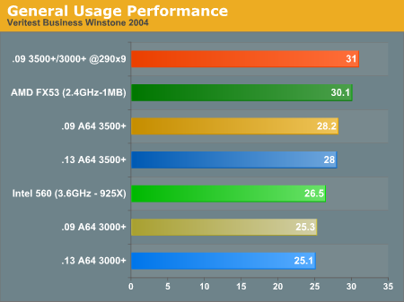
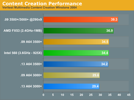
Because of the real world performance measured by the Winstone benchmarks, we did not really expect any difference between 90nm and 130nm results. However, the 90nm processors perform a bit faster than 130nm at the same speed in Business Winstone and Mutlimedia Content Creation Winstone. The differences are very small, but this is the beginning of even larger performance differences in Gaming benchmarks.
It is interesting that a 45% increase in clock speed (1.8GHz to 2.6GHz) on the 3000+ yields a 33% increase in Content Creation scores, but just 24% in Business Winstone. This is just another example showing that multimedia is much more impacted by CPU speed than standard Business applications.
Gaming Performance
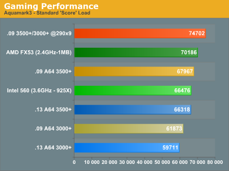
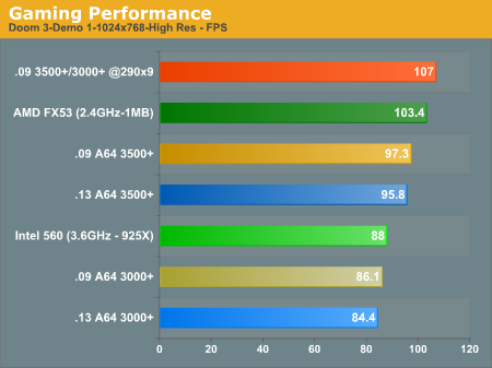
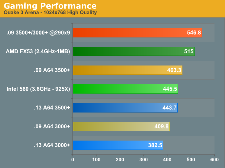
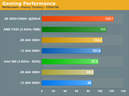
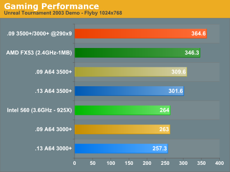
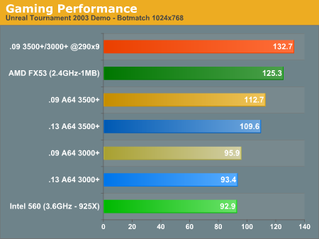
Gaming Performance was consistently faster on the new 90nm than the existing 130nm processors. This varied from 2% in Aquamark3 and Doom3 to 7% in Quake 3. Overall, gaming averaged about 3% faster on the new 90nm chips. While 3% is not a huge increase and it will likely not even be noticed by the average user, it was still impressive to see the new 90nm chips perform a little better than the older 130nm chips.
We have talked in past reviews about how some games respond well to CPU and memory speed increases, while others seem to be most influenced by the graphics card. This is nicely illustrated in comparing benchmarks of the 3000+ at stock speed to the same benches at 2.6GHz (290x9). Here, we see games like Return to Castle Wolfenstein, Unreal Tournament 2003, Quake 3, and Comanche 4 improve 34% to 42% as we move from 1.8Ghz to 2.6Ghz. At the other end of the spectrum, Halo and Aquamark 3 only improve 12% to 13% while the CPU speed increases 45%. Doom 3 falls in the middle with a 24% increase in frame rate for the 45% boost in CPU speed.
Final Words
We were impressed with the performance and overclocking that we found with the 90nm 3500+. However, it is very difficult to draw any conclusions based on a single sample, so we also bought a 90nm 3000+ from another vendor. These two processors, at different speeds and from different sources, performed similarly enough to allow us to draw some broad conclusions about the performance of the new 90nm Athlon 64 processors. The new 3500+, 3200+, and 3000+ perform from 1% to 7% faster than comparable 130nm parts. We still don't know if this is the result of the die-shrink or the new DH8-D0 revision. We checked all recent Athlon 64 in the lab and we could not find a D0 A64 for comparison. We have asked AMD to shed some light on what we found in our testing, and we will report what AMD says about the performance improvements as soon as we receive the information from AMD.Based on the Performance tests alone, there is reason to be pleased with what we know of the AMD die-shrink so far. If you also consider the fact that AMD appears to have accomplished the shrink to 90nm without an increase in heat, the process move should be considered a big success. We won't know this for sure until we see the fastest AMD chips in 90nm clothes - that is where the thermal impact of the shrink will be most visible.
The other side of the equation is headroom or overclocking. AMD enthusiasts have always seemed to flock to value chips in the AMD family. More than Intel users, AMD enthusiasts seem to always want something for nothing. It's not because they are cheap necessarily, but because AMD won them over by providing outstanding value points in their product line. In fact, many AMD users have hung on to Socket A technology long after it was significantly outperformed in the market because they could buy the Athlon XP cheap and overclock the heck out of it. Those users will love the new 90nm chips in general - and the 90nm 3000+ in particular.
They will love the new 90nm chips because they can buy a 3000+ running at 1.8GHz for less than $200 and still have a good chance of reaching 2.6GHz with very little effort with the same chip. 2.6GHz is faster than any current Athlon 64, and it is, in fact, the speed that we expect from the upcoming FX55 - the new Athlon 64 top-of-the-line. It's been a while since we've seen this kind of headroom on an AMD chip, and those who were waiting for 90nm to get a magic overclocker will get in line to buy the new 90nm 3000+.
The major impact of the new 90nm Athlon 64 chips may not be quite as obvious. Prior to the new 3000+, 3200+, and 3500+ 90nm chips, the entry point to dual-channel 939 was the $400 3500+. As a result, buyers saw the Socket 754 as the value solution for Athlon 64 shoppers, where they could buy a 754 Sempron 3100+ for about $120 or a full 64-bit 2800+ for around $140. The new 3000+ should cost about the same as the 130nm 3000+ once the new settles into the market. That will make the cost of entry for the top 939 chipset well below $200 for the CPU. Many buyers who would have bought 939 if it had been cheaper will now be able to buy 939.
This leads us to future directions for 754 and 939. Roadmaps show 754 ending in late 2005, but 5 quarters is still a lifetime in CPU sockets. AMD plans to discontinue Socket A and move all processors to Socket 754/939/940. This will likely mean that we will see even cheaper 754 processors to entice buyers who found Athlon XP prices attractive. 754 will likely move much lower before it goes away in a year or so, and 939 will also likely move down a bit further as 90nm is fully implemented and production costs go down. All-in-all, it's becoming a very good time to be in the market for an Athlon 64 processor.


