Original Link: https://www.anandtech.com/show/1098
AMD Opteron Coverage - Part 1: Intro to Opteron/K8 Architecture
by Anand Lal Shimpi on April 23, 2003 3:03 AM EST- Posted in
- CPUs
In AMD's entire history as a mainstream microprocessor manufacturer, they have never seen as poor execution as they did with the K5. After several months of delays, the chip finally hit the streets only to be a CPU that ran too hot and couldn't offer very competitive performance.
On the flip side, AMD had never seen their engineers on top of their game like they did during the days of the K7. What eventually became the Athlon microprocessor was truly a feather in AMD's cap; what ended up holding back the success of the K7 core was sheer marketing and politics - two things that even the best design teams out of AMD could not dream to control. Even with the disadvantages AMD was faced with, the K7 still went on to become the underdog's best effort to date - and thus when they announced its successor, the K8, at the Microprocessor Forum in 2001, expectations were very high.
We concluded our first article on AMD's K8 (aka Hammer) architecture in October of 2001 with the following:
AMD is clearly not the company it was a few years ago. They are constantly making steps towards becoming more of an industry leader as opposed to the follower they have been criticized of being for so long; the Hammer architecture is the most vivid depiction of what sort of an industry leader AMD is capable of being.
At the same time we shouldn't discount Intel as they still hold the majority of the market and they do have the potential to take their technology very far. What AMD's recent gains do prove however is that there won't be a return to domination for Intel anytime soon; this two man race will be continuing for some time to come. Both AMD and Intel have had their slipups; while Intel's have been more recently, AMD is far from immune to them.
The technology behind Hammer is there, as is the potential for it to succeed. But AMD has a lot of work to do between now and its release in the next 12 months. Many forget that until the Athlon, AMD didn't have the best execution track record. It's a long road ahead for the Hammer design team, good luck guys.
Fast forwarding to today, it's clear that AMD not only didn't hit their target release with Hammer, but the process was far from another K7 launch. We asked AMD's CTO, Fred Weber, to characterize the execution of the K8 launch and he fairly summarized it as not as good as the K7 but better than the K5/K6.
It has been a very long road for AMD; dealing with a new microprocessor architecture, never-before-used manufacturing process (Silicon on Insulator) and all while facing very tough competition from Intel and a weakening world economy. The light at the end of the tunnel is finally able to be seen, and although the K8 isn't going to be available on desktops for another several months, its workstation/server release is here and it's called Opteron.
This article will focus exclusively on the architecture of the K8 core and how it relates to Opteron, we have three other pieces published in tandem with this one that cover everything from enterprise performance to desktop performance of Opteron. Here are direct links to the other articles:
AMD's Opteron Coverage
- Part 2: Enterprise Performance
AMD's Opteron Coverage
- Part 3: 1U Server Roundup
AMD's Opteron Coverage
- Part 4: Desktop Performance
We strongly suggest reading this article in its entirety before proceeding onto the rest, unless you're already intimately familiar with the K8 microarchitecture.
With that said, and without further ado, let's get to it.
Designing a CPU, More Specifically the K8
When we first looked at the K8 around two years ago we noted that, architecturally, not much had changed from the K7. Many attributed this to the old axiom, "if it ain't broke, don't fix it," and to a certain extent they were correct. The K7 microarchitecture proved to be an excellent performer, and even to this day has managed to at least remain competitive with Intel's NetBurst microarchitecture found in the Pentium 4.
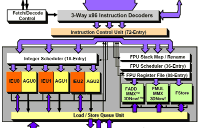
First let's take a look at the K7 block diagram:
Next, let's compare it to a portion of the K8 block diagram:
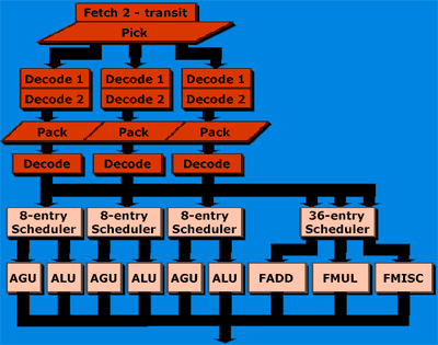
As you can see, the physical number of execution units remains unchanged from the K7. Remember that the K8 core has to be used as the base for both desktop and enterprise class processors, so "going wide" (meaning adding more execution units) wouldn't make an incredible amount of sense for the multipurpose nature of the K8.
The next thing to notice is that there are already indications of slight changes from the K7. Note that although the floating point units have the same medium-sided scheduling window (36-entry), the integer units are now fed by a larger set of schedulers (24-entry vs. 18 entry in the K7).
Why would AMD expand the size of the integer scheduling window of the K8 but leave the same number of execution units? For the answer to this, we have to look at the first limitation in how "big" of a CPU AMD can build - the branch prediction unit.
Building a Big CPU
It turns out that how "big" you can make a microprocessor (how wide - how many execution units, and how deep - how many stages in the pipeline) is first limited by the accuracy of your branch predictor. The branch predictor single handedly determines the number of instructions you can have "in flight" (active in the pipeline) before the CPU will incorrectly predict a branch, causing a stall in the pipeline. In theory, your CPU should be no bigger than it needs to be, thus it should be able to accommodate no more than the number of instructions that can be sent down the pipe before a mispredict will occur.
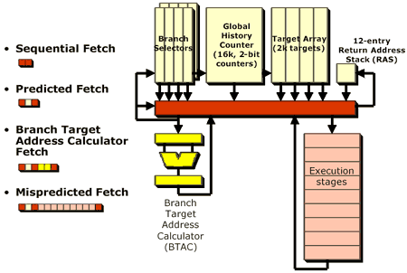
With the K8, AMD improved on the branch prediction unit of the K7. The global history counter has been increased tremendously, and is now four times the size of the global history counter in the K7. The global history counter is actually a massive array of 2-bit counters (2-bit counters count from 0 - 3) that actually determine whether or not a particular branch should be taken. When a branch instruction is reached, the branch prediction unit takes a part of the address of the instruction (and sometimes performs some logical operations on the address) and uses that as an index into the global history counter - this determines which counter to look at and increment. The counter at that index is examined, and if its value is greater than or equal to 2, the branch is predicted as "taken" and the branch is taken. If the branch was incorrectly predicted, then the value of the counter is decremented by one, but if it was correctly predicted then the value of the counter is incremented by one (remember that the counter does have set limits, it can't be decremented past 0 or incremented past 3 as it is only a 2-bit counter).
The problem with this approach is that if you have two branch instructions that are given the same index value, the counter associated with that index value will be arbitrarily incremented or decremented; this is known as interference. The larger your global history counter is (the more 2-bit counters it is composed of), the less likely interference will occur. And finally, the less interference you have, the more accurate your branch predictor will be.
There are some other improvements to the K8's branch predictor, but all of them result in an overall more accurate prediction of branches. Going back to our original statement that the accuracy of a microprocessor's branch predictor determines how big we should build our CPU, by outfitting the K8 with a more accurate branch predictor, AMD enabled the K8 to be a bigger CPU than the K7; but bigger how?
Go Deep
At this point, AMD had two options - go wide, or do deep. To go wide would mean to increase the number of execution units in the core, which would make sense if the K8 were to be an enterprise-only core as a wider core is better suited for massively parallel applications. However, the desire to make K8 a desktop solution and the resulting desire for higher clock speeds led AMD to go deep, that is, deepen the pipeline.
Regardless of what route AMD chose, one thing was for sure; in order to take advantage of the fact that more instructions would be coming down the pipe between branch mispredicts, they'd need a larger buffer to store these instructions in. The buffer that keeps instructions "in flight" is known as the scheduling window, and if you look back up at the increase in the number of entries for the integer scheduler you'll now understand why AMD made the change; more instructions in flight, requires more entries in the schedulers to keep up. We can only assume that the floating point scheduling window was already large enough that it did not need any expansion; keep in mind that most branch instructions occur in integer code, which would help explain why the floating point scheduler remains unchanged from the K7 despite the more accurate branch predictor.
|
AMD
Integer Pipeline Comparison
|
||
|
Clock
Cycle
|
K7
Architecture
|
K8
Architecture
|
| 1 |
Fetch
|
Fetch
1
|
| 2 |
Scan
|
Fetch
2
|
| 3 |
Align
1
|
Pick
|
| 4 |
Align
2
|
Decode
1
|
| 5 |
EDEC
|
Decode
2
|
| 6 |
IDEQ/Rename
|
Pack
|
| 7 |
Schedule
|
Pack/Decode
|
| 8 |
AGU/ALU
|
Dispatch
|
| 9 |
L1
Address Generation
|
Schedule
|
| 10 |
Data
Cache
|
AGU/ALU
|
| 11 |
Data
Cache 1
|
|
| 12 |
Data
Cache 2
|
|
So AMD opened up the integer scheduling window, and gave the K8 a couple more pipeline stages to play with. The purpose of these additional stages, as we mentioned before, is solely to allow the K8 core to reach higher clock speeds. The more pipeline stages you have, the less work is done per clock and thus the higher you're able to clock your CPU; this is the reason the 20-stage Xeon is currently at speeds of 3GHz, compared to the 12-stage Opteron which is debuting at 1.8GHz.
The difference in pipeline architectures is what makes a clock-for-clock comparison between the Xeon and Opteron invalid (much like the Pentium 4 to Athlon XP comparison was invalid on a clock-for-clock basis). The Xeon's architecture allows it to reach high clock speeds at the expense of doing less work per clock cycle, the appropriate comparison ends up being one of cost and real-world performance, not one of clock speed.
The K8 caches are identical to the K7 caches, although with slightly lower latencies and higher bandwidth as you can see from the following performance comparisons:
|
|
|
|
The final microarchitectural changes (before we get into the two big ones) to the K7 core come in the form of what AMD likes to call the K8's "Large Workload TLBs."

The number of entries in the K8's Translation Lookaside Buffers has been increased in order to cope with the usage model the Opteron will most likely find itself in - servers with very large memory requirements. The performance impact of the increase in TLB entries on the desktop will most likely be minimal as we noticed when AMD first increased TLB sizes with the K7 Palomino core; 3D rendering applications did receive a somewhat reasonable performance boost if you recall.
AMD's 64-bit strategy - x86-64
We have yet to talk about a fundamental part of the K8/Opteron architecture - 64-bit support. The K8 is the world's first and only 64-bit x86 core, the reason it is the only such core is because AMD came up with the 64-bit extension to the x86 instruction set.
In the past, Intel had been the ones to extend the x86 ISA (Instruction Set Architecture) beyond its 8-bit foundation. But once Intel hit 32-bit and started to look towards the future and 64-bit microprocessors, they wanted to rid themselves of the somewhat bulky x86 ISA and move towards something much more robust - and thus, IA-64 was born.
The IA-64 ISA is significantly better than the x86 ISA in a number of ways, but the discussion of IA-64 is beyond the scope of this article as we're here to focus on x86. The biggest problem with the IA-64 ISA and thus IA-64 microprocessors is the lack of native x86 compatibility, effectively keeping IA-64 processors from running over two decades worth of software. Intel recognized this and equipped their IA-64 processors (Itanium, Itanium 2, etc…) with an x86-to-IA-64 decoder, that takes x86 instructions and decodes them into IA-64 instructions. This decoder is not the most efficient decoder nor is it the best way to run x86 code (the best way would be to run it natively on an x86 processor), and thus the Itanium and Itanium 2 offer quite poor performance under x86 applications.
The benefits of a 64-bit microprocessor architecture are mainly memory related; if you take two identical microprocessors, make one 64-bit and one 32-bit, the advantage of the 64-bit CPU is that it can address much more memory than the 32-bit CPU (2^64 vs. 2^32). For those that were hitting the limits of 32-bit memory addressability (4GB), Intel's only high performance solution was to transition to Itanium, but if all you're looking for is more than 4GB of memory and solid x86 performance, then you're SOL from Intel's perspective.
AMD's 64-bit strategy is significantly different; AMD has always been focused on the current customer needs, not on the vision of the computing future 5 - 10 years from now and this is reflected in their 64-bit strategy. The strategy is simple and has been done before in the past; stick with a high-performing x86 core, and simply extend the ISA to support 64-bit memory addressability - the end result is what AMD likes to call x86-64.
The features of x86-64, whose implementation in Opteron is called AMD64, are pretty straight forward:
1) backwards compatible with current x86 code
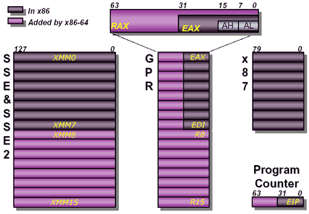
2) 8 new 64-bit general purpose registers (GPRs) as well as 64-bit versions of the original 8 x86 GPRs (only available in 64-bit long mode, described below)
3) SSE & SSE2 support along with 8 new SSE2 registers
4) Increased memory addressability for large dataset applications (only available in long mode, described below)
5) Solid performance in current 32-bit applications with support for 64-bit applications going forward, a good transitional processor
With the ability to run current x86 code as well as future x86-64 code, you can guess that the K8 has two operating modes; they are called "legacy" and "long."
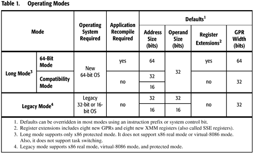
In legacy mode, the K8 will run all native 16 or 32-bit x86 applications, the processor basically acts just as a K7 would.
Things get interesting in "long" mode where a 64-bit x86-64 compliant OS is required; in this mode, the K8 can either operate in full 64-bit mode or in compatibility mode. Full 64-bit mode allows for all of the advantages of a 64-bit architecture to be realized, including 64-bit memory addressability. One of the major features of the K8 architecture is the fact that the number of general purpose registers is doubled when in x86-64 mode, and thus this feature is also taken advantage of in full 64-bit mode.
Compatibility mode gives you none of the advantages of a 64-bit architecture on the application level, as it is designed for running 32-bit apps on a 64-bit OS (hence the name compatibility); The extra registers and 64-bit register extensions are ignored in this mode. Compatibility mode is important because of the 2GB process size limitation under Windows OSes. Although 32-bit Windows offers support for a maximum of 4GB of memory, each process can only use a maximum of 2GB of memory - the remaining 2GB is reserved for the OS. By running a 64-bit version of Windows (when released) and a 32-bit application, compatibility mode allows for each 32-bit process to have up to a full 4GB of memory, with the OS using anything above that marker.
Finally we have 64-bit long mode, where there is more than meets the eye. In addition to > 4GB memory addressability, in 64-bit long mode, applications have access to twice as many named general purpose registers. Remember that registers are basically high speed memory locations on the microprocessor where temporary values are stored. For example, if you were to compute the sum of two numbers, both of those numbers as well as the final result would be stored in these registers.
The problem you run into however is what happens when you run out of registers. You can't simply add more registers because older applications compiled with support for your instruction set architecture would not be able to recognize the new registers; if your ISA is originally designed with 8 registers, you're stuck with those 8 registers unless you change the ISA - something that doesn't happen too often as it tends to break backwards compability unless you take an AMD x86-64 route of extending the ISA, in which case you're still unable to offer more registers to older applications not compiled with the updated ISA in mind.
When you do run out of registers, there's no other option than to use main memory (or cache) as scratch space to store the temporary values. Unfortunately even going to cache is wasteful when compared to storing data in these high speed memory locations, and thus it is imperative that you store data in registers as often as possible. The more registers you have, the less likely you're to run out of them; it's as simple as that. The doubling of the number of registers definitely helps overall performance, assuming you're running a 64-bit OS and have applications that are compiled in 64-bit long mode to take advantage of the added registers.
Look what we found, an on-die memory controller
One of the most controversial decisions behind the K8 core was to integrate the majority of the North Bridge functionality on-die, including the memory controller.
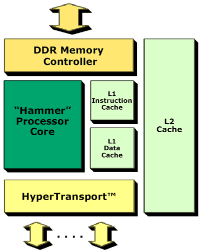
The Opteron features a 144-bit wide DDR memory bus, meaning that 72-bit (64-bit + 8 parity bits for ECC memory) DIMMs must be installed in pairs. As the bus widths allude to, the Opteron only supports registered ECC DDR SDRAM.
The benefits of an integrated memory controller are clear - low latency memory accesses and an extremely fast controller design thanks to the fact that it is manufactured using the latest processes using the fastest transistors.
|
You can see that the integrated memory controller of the Opteron is significantly lower latency than the nForce2's dual-channel DDR memory controller. It is also worth noting that the 875P memory controller is extremely low latency, especially for an external controller - but you have to keep in mind that we're comparing two different clock speed CPUs here when we're comparing to the Intel platform. While the platform may have a latency similar to that of the Opteron, the CPU is running at a much higher frequency meaning that more clock cycles are being wasted in the same amount of time:
|
The above graph shows the number of clock cycles wasted on waiting for data from main memory, here we see the clear advantage of having an on-die memory controller.
The downside to the on-die memory controller is that in order to get support for new memory technologies, you need to replace your CPU, not just your motherboard. AMD has built functionality into the K8 core that allows an external chipset to disable the on-die memory controller and use an external one. However, remember that a K8 without the integrated memory controller is basically like an optimized K7 with a longer pipeline.
Multiprocessor Mecca
Whereas the K7 was architected to be AMD's flagship desktop processor, the K8 was designed from the start to be an excellent enterprise processor with versions eventually trickling down to the desktop. With this in mind, it makes perfect sense that the K8 core should be well suited for multiprocessor environments.
To understand how the K8 (and Opteron) are so perfectly tailored to MP environments you have to first understand the limitations in conventional architectures. The Athlon MP brought to light the first limitation of conventional MP Intel architectures - the shared FSB. Regardless of whether you had one, two or four processors, they all shared the same 64-bit wide FSB that connected the CPUs to the rest of the system. The obvious bottleneck here is that the more CPUs you have, the less FSB bandwidth each individual CPU gets.
AMD got around this limitation with the Athlon MP by giving each CPU its own 64-bit connection to the North Bridge, introducing the world's first point-to-point FSB protocol used on an x86 machine. AMD's approach was higher performing than Intel's, but at a much higher cost; the 760MP chipset was an extremely expensive chipset, and that's only for a 2-way setup. AMD never built a 4-way Athlon MP chipset, mainly because of a lack of demand, but it wouldn't have been very easy had there been tremendous demand for the solution.
With the K8, AMD took things one step further and offered an even higher performing MP solution that was also cheaply scalable courtesy of a technology AMD pioneered called Hyper Transport. Hyper Transport is a serial point-to-point bus that AMD uses to connect everything from I/O controllers to AGP/PCI bridges and even CPUs.
The Opteron features three 16-bit wide HT links, with each link offering up to 3.2GB/s of bandwidth in each direction (for a total of 6.4GB/s of bandwidth per link). Each Opteron CPU can connect to other Opteron CPUs using two of the three links, the third link is present for any I/O chips that the CPU must connect to.
|
The
Multiprocessing Capabilities of Opteron
|
||


The beauty of this setup is that a configuration of 8 CPUs is just as easy to implement as a configuration of 2 CPUs, no need for expensive chipsets.
A side effect of each CPU having its own memory controller is that memory bandwidth scales with the number of CPUs you have present. Whereas in conventional MP architectures CPUs must share the memory bandwidth much like they do FSB bandwidth, with Opteron, each CPU gets a dedicated 128-bit DDR memory bus to itself. With multiple CPUs in a system, each CPU can use both its own memory controller as well as a non-local memory controller to pull in data, thus increasing effective memory bandwidth even further. For example, the Opteron supports a maximum of DDR333 SDRAM currently, giving it a peak bandwidth of 5.3GB/s per CPU. The CPU can also pull data from other memory controllers in a n-way machine as quickly as 3.2GB/s, the maximum transfer rate of the HT link between two CPUs.
In order for the performance benefit of this sort of memory access to be truly taken advantage of, the OS needs to be smart enough to not put all data in the first xxxMB of memory. Instead, the OS must keep data in memory in such a way as to optimize for local and non-local memory accesses. For example, in a 4-way Opteron server with each CPU having 1GB of memory, if the working dataset is only 512MB in size it shouldn't all be placed in CPU0's memory - especially if all four CPUs are using the data. It should either be copied to all four sets of memory, or it should be divided up so that all CPUs can have at least some local access to the data at their full 5.3GB/s rate. This type of memory access is known as NUMA, which stands for Non-Uniform Memory Access; Windows 2003 Server supposedly has support for NUMA.
The culmination of all of this is that the K8 core (and thus the Opteron) scales very well with the number of CPUs you have in a system, much better so than any Intel processor. To prove this we've taken an excerpt from one of our tests in Part 2 of our Opteron coverage and compare the benefit of moving to dual processors from an Opteron standpoint vs. a Xeon standpoint:
|
Whereas the Xeon only sees an 11% increase in performance from going to two CPUs, the Opteron sees an impressive 24% performance boost! These are not numbers to scoff at; AMD has clearly designed the Opteron for serious multiprocessing environments. We hope to be able to bring you 4-way scaling benchmarks very soon.
Another interesting thing about the K8 architecture is that it has already been engineered for use in multicore designs. AMD's Fred Weber mentioned to us that the logic for multicore, single die Opteron processors has already been verified, although nothing has taped out. The process is actually quite simple; AMD produces two Opteron cores, removes the physical layers of the Hyper Transport links and connects the two on a single die. AMD could do this today if they desired, however according to Mr. Weber, a multicore Opteron only makes sense if they can keep their die size below 120 mm^2. Two Opertons on a single die at below 120 mm^2 will be possible on AMD's 65nm process, so whenever that transition occurs you can expect to hear a bit more from AMD on multicore Opteron solutions.
Let's get physical
Thus far we've focused on the core architecture of the Opteron, but there's much more to a CPU than the microarchitecture.
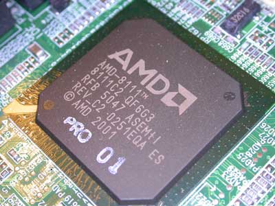
The Opteron is built on AMD's most advanced manufacturing process to date - a 0.13-micron process featuring Silicon on Insulator (SOI). Additional frequency headroom and cool running operation are both positive benefits of SOI, for more information on what SOI is be sure to read our quick one-page explanation of it here.
Thanks to its 1MB L2 cache on top of its already complicated die, the Opteron is AMD's biggest and most expensive chip to manufacture - with a die measuring just under 200 mm^2. AMD has told us in the past that their manufacturing sweet spot is around the 100 - 120mm^2 mark; it's clear that AMD isn't having much fun making Opteron.
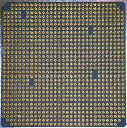
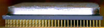
The expensive chip continues to be a nuisance to manufacture once you look at the underside of the CPU, at all 940 pins. The packaging costs alone are higher than anything AMD is used to, thanks to the three HT links and 128-bit wide memory interface present on every Opteron CPU (this partially explains the very high pricetag of Opteron processors).
Interestingly enough, AMD has reverted back to using a ceramic package with the Opteron rather than the organic packaging introduced with the Athlon XP. AMD will certainly have to migrate to organic packaging as clock speeds increase, but we have a feeling that the benefit of reduced current draw courtesy of SOI has enabled AMD to stick with a ceramic packaging where they couldn't otherwise.
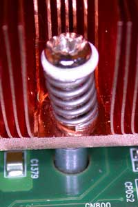
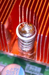
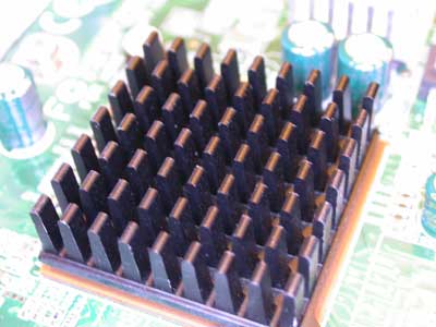
An excellent heatsink mounting mechanism
Mounting heatsinks has become a dreaded task in recent times, mainly because of poorly designed solutions that could pose danger to either your CPU or your motherboard, or even both.
Even Intel has fallen behind as the latest Pentium 4 coolers have a tendency to bend the motherboard's PCB because of the mounting mechanism and the incredible amount of force required to keep the heatsink mounted properly.
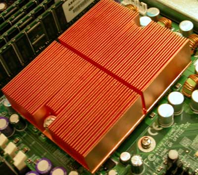
AMD's solution for Opteron is quite elegant and requires no more than two screws:
 |
 |
Thanks to the integrated heatspreader on the Opteron, we no longer have to worry about cracked cores:
Sigh, Opteron Nomenclature
When AMD launched the Athlon XP, we were huge fans of the processor but had serious issues with AMD's naming system. AMD's modeling system has been relatively successful from the standpoint that very few users seem to know (or care?) what clock speed their Athlon XPs are running at, and refer to their processors solely by model number. One major flaw with AMD's model number system was that Athlon MP processors, AMD's K7 based server/workstation CPUs, received model numbers based on performance in desktop applications; with the Opteron, AMD has finally divided how they model desktop and server/workstation CPUs.
The Opteron modeling system consists of a simple three digit number, xyz. The first digit, x, indicates the total number of these processors you can use in a SMP system. For example, a 200 series Opteron could be used in both 1-way and 2-way systems, whereas an 800 series Opteron could be used in 1-way, 2-way, 4-way and 8-way systems.
The remaining digits, yz, are relative performance indicators, with little information given to exactly how they are derived. All we know is that an Opteron x44 is faster than an Opteron x42, but that could be because of clock speed, cache size or Hyper Transport link speed among other things; like it or not, it's what you'll have to deal with.
AMD is launching three Opteron flavors today, two of which should be available at the time of publication with the highest clocked offering seeing mass market availability in June.
|
AMD
Opteron Model Numbers
|
|||
| CPU Name |
Clock
Speed
|
||
| Opteron 244 |
1.80GHz
|
||
| Opteron 242 |
1.60GHz
|
||
| Opteron 240 |
1.40GHz
|
||
As we've mentioned before, the Opteron is launching at 1.4, 1.6 and 1.8GHz, carrying model numbers 240, 242 and 244 respectively. There are no differences between the three model numbers other than clock speed.
What's interesting to note is that AMD has hit higher frequencies than 1.8GHz on their non-SOI 0.13-micron process (remember the Athlon XP 2800/3000+ both run at above 2.0GHz), which leaves us wondering why AMD chose to launch at such conservative frequencies with Opteron. It could either be that hitting higher frequencies is going to take a little more effort because of kinks in the 0.13-micron SOI process, or AMD is attempting to launch with as low a clock speed as possible yet still remain competitive in order to effectively save their strength for when it's absolutely necessary.
Opteron Chipsets
We have seen a plethora of chipsets for the forthcoming Athlon 64, but for Opteron there didn't seem to be that much support outside of AMD's own solution.
The AMD 8000 series works just as well with the Opteron as it will with the Athlon 64, and that's the chipset you'll see on virtually all Opteron based systems. Because AMD is focusing this launch on the enterprise market, none of the current Opteron boards feature AMD's 8151 AGP Tunnel, thus we have no AGP slots on any of the Opteron boards we have our hands on.
The AMD-8111 HyperTransport I/O Hub (aka South Bridge)
The AMD-8131 HyperTransport PCI-X Tunnel
Opteron Chipsets Continued - Introducing nForce3 Professional
Talk about taking everyone by surprise, NVIDIA has marked an early entry into the K8 chipset market with their nForce3 Pro chipset.
A single chip solution, the nForce3 Pro is aimed at the 1P Opteron workstation/enthusiast market - and yes, the chipset does have an integrated AGP 8X controller.
Launching today is the nForce3 Pro 150; since the Opteron already has the memory controller taken care of, NVIDIA really only had to integrate their AGP, Ethernet, IDE and sound controllers on a single chip to make the chipset complete. The nForce3 Pro 150 features 8X AGP support, NVIDIA's 10/100 MAC (virtually identical to what's in the nForce2) and basic AC'97 audio support (no APU). The Pro 150 supports three Ultra ATA 133 channels, with the third channel able to hook up to a Serial ATA bridge in order to bring non-native Serial ATA support to the chipset today. Because of the target market for the chipset, the nForce3 Pro 150 does not feature any integrated graphics.
This Fall you'll see the introduction of nForce3 Pro 250, with support for Gigabit Ethernet (NVIDIA's own Gigabit MAC) and Serial ATA (two ports native). The nForce3 Pro 250 will continue to be a single chip solution, and NVIDIA is stating that their internal pathways connecting the Gigabit controller to the Hyper Transport link will be wide/fast enough as not to be a bottleneck.
You can probably guess that the Athlon 64 chipset will most likely be called nForce3, with the Pro tag being reserved exclusively for the workstation market.
ASUS is NVIDIA's sole launch partner with nForce3 Pro and they will have boards available in the next two months.
Final Words
After two years of waiting, we finally have hardware to back up all the claims AMD has been making with regards to Opteron. We are still several months away from the desktop release with Athlon 64, but as you'll see from our other articles, the performance could be worth waiting for - assuming AMD can ramp up clock speeds.
The Opteron has the architecture behind it to threaten Intel's Xeon line, but when pulled off the paper and placed in the real world, can AMD put the money with their mouth is? Find out in Part 2 of our Opteron coverage where we benchmark the CPU in enterprise environments…


