Original Link: https://www.anandtech.com/show/876
Inside Intel: From Silicon to the World
by Anand Lal Shimpi on February 11, 2002 3:58 AM EST- Posted in
- CPUs
Almost as absurd as the idea of Intel backing out of their IA-64 development
in favor of x86-64 is the unfortunate perception that the world’s largest desktop
microprocessor manufacturer is not driven by engineering but rather by marketing.
If microprocessor design were easy enough for a team of PR agents to tackle
then many of us would have to change majors or head back to school very soon.
The fact of the matter is that Intel is as driven by innovation as they are
by engineering and in order to get an idea of what exactly goes on inside
Intel, we made a trip up to the Intel Labs in
This article won’t cover any NDA information, it won’t reveal secrets about Intel’s roadmaps for 2002, rather it will serve as a bit of insight into how Intel operates at the engineering level. The Intel you normally hear about is the Intel that’s pulling balloons down at Computex or the Intel that’s suing VIA for something or other, today we’ll be showing you the Intel that doesn’t care about anything outside of making fast, reliable and powerful circuits.
An Engineer’s Playground – Intel Labs
Our first stop at Intel was at their Labs. The Intel Labs are quite possibly the most interesting arm of Intel as they have no PR or Marketing group and they aren’t product driven. The group is entirely technology driven meaning that their very talented engineers go to work every morning to test theories and ideas. Eventually these theories and ideas may make their way into products but this group isn’t concerned with selling more Pentium 4s, they are focused on pushing the limits of technology.
At Fall IDF 2001 we mentioned a 5GHz, 32-bit ALU that Intel was demonstrating. That accomplishment came courtesy of the Intel Labs.
Much more than simply performance tuning comes out of these research labs however, there are actually five main focus areas for this group:
1) Performance – This area is pretty much straightforward, the group is constantly looking for ways to increase clock speed and perform computations more efficiently. They also look at application usage trends and algorithms in order to help decide how the next-generation of microprocessors should work and how to optimize them for the types of loads and application usage that the end-users are actually encountering.
2) Power – The biggest challenge going forward in microprocessor design is combating the issue of power consumption and heat dissipation. It turns out that power and performance end up going hand in hand meaning that as one problem is tackled, improvements in the other are usually opened up.
3) Integrity – Having reliable processors is something we almost always take for granted, but reliability is a very difficult thing to ensure especially when you’re dealing with hundreds of millions of transistors packed extremely tightly into a space the size of a dime. Research into making more reliable circuits under various conditions is also a duty of these labs.
4) Functionality – We mentioned earlier that much research time is devoted to studying application behavior, a major part of the results of those studies is incorporated into execution units that make their way into future CPUs or even lower-level improvements that deal with moving data around internally, optimizing data paths for certain types of transfers, etc… Technologies such as MMX, SSE, SSE2 and HyperThreading were the results of this type of research from within the labs. A number of other technologies that were never given marketing names were also the results of their efforts in the labs but those are even more improvements that are generally taken for granted.
5) Tools & Methods – The final focus of the group is on developing things like simulation tools that better help in the other four areas we just mentioned.
Now that you understand a bit of what the Intel Labs are about, it’s time to talk about some of the things they’re working on right now.
A Menu of Technologies
Keep in mind that the main goal at the Intel Labs is to create a menu of technologies that the product and design engineers can then select from to include in the products that they’re making for the future. For example, IAL engineers may design a double-pumped ALU in order to test out a new circuit theory, this double-pumped ALU may eventually get included (in one shape or another) in a processor such as the Pentium 4.
We use the ALU example because that happens to be a very common thing to experiment with in the labs. The reason being that it’s pointless to spend design time working on circuits that have no purpose, but by creating a useful set of logic such as an ALU not only do the technologies that went into its production get tested, but the ALU itself can then be later used in products.
One such technology that the engineers have been working with and were eager to discuss upon our visit was the idea of adaptive body biasing transistors. There is an incredible amount of math and analog circuitry that goes into the idea of body biasing transistors but the simple $0.10 version of the story is that by controlling the voltage applied to the body of a transistor you can cause the transistor to switch either faster or slower. By applying a positive body bias you can make the transistor switch faster, normal bias will make the transistor switch at the same speed, and zero bias will make the transistor switch slower.
Adaptive body bias is the dynamic adjustment of body bias on transistors depending on how fast or how slow they’re switching. This seems like a simple thing but its applications are numerous. Remember that the speed of a complex circuit is dependent on the speed of its slowest part. For example, if you have a circuit whose transistors are capable of switching at 10GHz but a small portion of them can only switch at 8GHz, your circuit (e.g. CPU) will be limited to 8GHz. Using by applying an adaptive body bias to the slower transistors it may be possible to speed them up to the speed of the rest of the circuit at 10GHz. This can have a huge impact on yield as it will be easier to get more transistors to run at higher frequencies. Especially moving forward as CPUs begin to have hundreds of millions of transistors, the likelihood of some not switching as fast as the rest increases. Adaptive body biasing will help tremendously in situations like these.
Improving Adders
The next type of technology that interested us was a brand new adder circuit. An adder circuit is obviously used in the integer addition of numbers and is a critical part of any CPU located in the ALU. When adding two numbers together in most of today’s CPUs the addition is performed using what’s known as 2’s complement addition. How is this any different from normal addition? It’s not really when you’re just adding two positive numbers; the numbers are added bit by bit so if we had two 4-bit numbers, 2 and 4 they would add like this:
| 0 | 0 | 1 | 0 | |
| + | 0 | 1 | 0 | 0 |
| = | 0 | 1 | 1 | 0 |
The need for 2’s complement addition comes into play when you’re dealing with negative numbers. We’ll spare you the details of why this is done but when finding the negative or complement of a number using the 2’s complement method you simply take the positive number, flip all the bits, and add 1. For example, the answer we got before, 6, negated would be:
| 0 | 1 | 1 | 0 | (6) | |
| 1 | 0 | 0 | 1 | ||
| + | 1 |
| = | 1 | 0 | 1 | 0 | (-6) |
Why is this important? Say your extremely fast processor is adding away and all of the sudden it has to subtract a number. The processor must stop what it’s doing and find the 2’s complement of that number before it can continue adding. With processor pipelines getting longer and longer, such a stall would wreak havoc on performance. So modern day ALUs use what is known as Dual Rail Domino logic for their adders.
The theory behind a Dual Rail Domino adder is that you should compute the complement of a number in parallel with the actual computation of that number. Then if you have to subtract a number you don’t have to wait until the complement is calculated as it’s already ready for use. The problem with this approach is obvious; you need to have twice the amount of circuitry to implement a single adder as well as an adder circuit to calculate the complement in parallel.
The Pentium 4’s double-pumped ALUs are actually only 16-bits wide, thus requiring a single clock to produce one 32-bit result. It’s fairly obvious that Intel will be moving to 32-bit ALUs in the future (considering that all the high-speed ALU demos we’ve seen have been of 32-bit ALUs) which will mean that they will have even more circuitry to include in processors to calculate larger 32-bit integers and larger 32-bit complements.
Necessity is the mother of invention and thus Intel has come up with a way to reduce the size of their dual rail domino adders. Obviously the methods employed in reducing the size of the complementary adder circuit are held pretty dear to Intel so they aren’t readily revealed. They call their reduced size implementation a Complementary Signal Generator (CSG) because of its function as logic that generates the complement to a number represented through a signal. Intel’s CSG is lower power than conventional designs and uses fewer transistors which will be a bigger issue as they move towards higher-speed multi-GHz 32-bit ALU designs.
Air-Cooled @ 10GHz, today
The culmination of these aforementioned technologies was in an air-cooled 10GHz 32-bit ALU running at room temperature:

A 10GHz clock frequency

The ALU's clock signal, it's not as smooth because of the exposed environmental
conditions

Click to Enlarge - The test setup, there's a 10GHz ALU in there
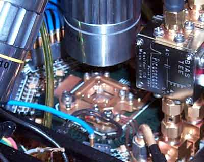
Here's the ALU.
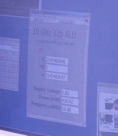
Proof that it works, try adding 1 to 2147483646 at 10GHz
Multi-core CPUs: The Intel Way
Over the past decade the focus in improving CPU performance has been on extracting as much instruction level parallelism (ILP) out of code as possible. The idea behind ILP is to execute, in parallel, as many instructions as possible. This keeps execution units busy and it makes computing efficient.
There is only so much ILP that can be exploited before you begin to receive diminishing returns. This is why CPU manufacturers are looking towards ways of improving performance through thread level parallelism (TLP), or the execution of as many threads in parallel as possible. Both AMD and Intel are working on methods of improving TLP; AMD is rumored to be testing a multi-core version of their Sledge Hammer processor and Intel has more recently introduced Hyper-Threading Technology which allows for the simultaneous execution of threads on a single processor.
Intel’s labs are also hard at work at discovering the feasibility of a multi-core CPU. The “simple” approach would be to have two identical cores running in parallel in a single package, however as we’ve outlined in the past there should be much emphasis on the packaging part of the equation. Intel has been toying with an interesting, more elegant approach.
With an increased focus on power consumption, Intel’s engineers have been hard at work in finding ways to make sure that future generations of processors won’t require water or other extreme cooling measures. And having two cores running in parallel will definitely make power consumption and dissipation very big issues, very quickly.
Intel’s theory revolves around having two cores, but not necessarily of identical characteristics. It turns out that a good part of the time your CPU is waiting for things like your disk drive or main memory and thus isn’t gaining much from running at full speed. Thus if you had two cores, one high-performance and one lower-performance you could save power and potentially even transistors if some functionality was removed from the lower-performance core. The high-speed core would be used for critical data execution and the other for execution of data that more dependent on slower paths such as from main memory or disk subsystems. Obviously there have been no products announced to feature this type of technology but Intel’s early findings show that the technology is promising. Remember that the labs aren’t product driven, rather technology driven so they’re not working on any particular products per se, just ideas that may end up taking shape in future products; it’s interesting nonetheless.
Intel’s Other Role: The CPU Doctor
Moving on past the world of neat ideas that are years away we journeyed to the present. One of the things we take for granted whenever we upgrade to that Athlon XP 2000+ or Pentium 4 2.2GHz processor is all the time and effort that went into the processor’s design and development. We’ve already introduced you to some of the development that goes on architecturally but what about the critical 6 - 8 months before a CPU is brought to market?
When a CPU design finally gets made into a piece of silicon, this silicon is known as an A0 stepping core – the first revision of the core that’s ever made. Before anyone gets to plug it into a motherboard and run it, it is sent off to a group of Intel lab technicians whose job is to try and uncover any problems with the processor.
There’s very little we can show you pictorially about this process because of the proprietary nature of some of the devices Intel uses but we’ll try our best to describe it to you.

This is the furthest our cameras would go, what's beyond these doors is quite
interesting.
Problems in this A0 silicon are detected using what is known as a Laser Voltage Probe (LVP) whose name clearly explains its function. One of the Intel lab engineers referred to it as a glorified multimeter which is pretty close to the truth. The probe is contained within a very large machine that examines portions of the silicon and compares the wired logic to the way the processor is supposed to behave at that point in the silicon. For example, a LVP operator would sit at a workstation and control the position of the probe on the die. Upon coming to a part of the die the operator would like to examine he/she will be presented with waveform data on how that particular circuit operates taken via the probe, as well as actual pictures of the transistors that the probe is “looking” at. Alongside all of this, the operator is given a complete logic diagram of the processor to act as a reference of what the probe’s seeing. So instead of seeing a random group of transistors with certain waveform data the operator is able to compare that to a symbolic circuit diagram to help determine the problem.
After a problem is determined, the chip architects are called back in and informed of the problem. They then go to work on a fix to hopefully solve the problem. But instead of throwing out the bad silicon and producing an entirely new chip with what should fix the problem, Intel has a way of performing “surgery” on an existing piece of silicon that rapidly speeds up development time.
If there’s a problem with the wiring in your car you can usually do the re-wiring yourself, because you’re dealing with wires that are inches or even feet in length and are easily accessible (relatively speaking). But what happens if there’s a problem with the wiring inside of a CPU? Instead of dealing with wires that are inches long you’re forced to deal with wires that are 0.03 microns in length. Even if you could somehow get access to the silicon without damaging it you wouldn’t be able to even begin to find the wires you’d need to add or remove in order to fix a problem with the circuit.
There’s another proprietary tool that Intel uses in order to fix these very types of problems – it’s called a Focused Ion Beam (FIB). The FIB tool is another large machine that takes a piece of silicon and instead of detecting problems with it the tool can be used to fix problems.
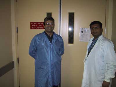
Our two Intel guides reminded us about the no-camera policy beyond the FIB doors.
Let’s say that using the LVP we mentioned earlier one of the operators discovers that the CPU has an extra NAND gate that must be bypassed. In order to bypass it, the input lines coming into the NAND gate and the output line leaving the gate must be cut, and a new connection must be made between those wires.
In order for the FIB tool to have access to the part of the silicon that it will be operating on the core itself must be shaved down to around 1.7 microns in height. This obviously must be done with the utmost care otherwise the core may develop stress fractures and be completely ruined in the process. Intel has another set of tools that preps the core for use with the FIB tool.
Once in the machine, the FIB can begin cutting wires and inserting new ones through the command of an operator sitting at a workstation. Depending on the complexity of the circuit repair being performed an average operation can take anywhere from a few hours to multiple days; all this just to add or remove a wire that’s hundredths of a micron in length. Keep that in mind the next time you get upset that AMD or Intel delays the release of a new CPU.
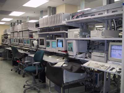
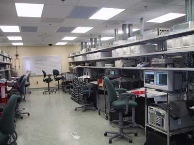
Intel’s Validation Labs
One of the things Intel is known quite well for are their Validation Labs. Many will argue that the price premium you pay when purchasing an Intel CPU over the competition is all of the time and effort that goes into validation; whether or not its worth it is up to the buyer to decide, but there is good reason that Intel’s corporate penetration has been so great historically.
There are two major parts of the validation labs, Intel’s SV and CV Labs which stand for System and Compatibility Validation respectively. The SV labs focus on validating a CPU (or CPUs) for use with platforms. So when Intel says that a CPU is validated for use in dual processor systems they mean that they have performed their extensive testing on the CPU in that configuration.
The CV labs are more end-user oriented as they focus on application compatibility with Intel products.
Intel’s System Validation Labs
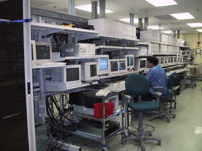
In the SV lab we were touring (there are many), the lab engineers were running a barrage of tests (developed in-house) on forthcoming Plumas solutions in single and multiprocessor configurations.
These systems are validated using test scripts that generate over 1 million tests per day. For every CPU and chipset that is validated Intel ends up performing approximately 1 billion tests in their SV labs. From what we’ve been told, this is the most rigorous set of validation requirements that any chipset vendor imposes on their products which may explain why Intel is often much later to the game when introducing new features such as DDR or PC133 SDRAM support.
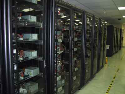
The testbeds go here

These computers feed data to the testbeds

This hall is filled with thousands of computers that are constantly testing
Intel platforms and products.
These tests are fed to the platforms via thousands upon thousands of computers running distributed computing applications to hammer the platforms. All errors are recorded and investigated until the source of the problem is found and resolved.
Intel’s Compatibility Validation Labs
After a platform makes it through the SV labs, it’s tested in the CV labs in a manner much more like what an end-user would encounter. The types of tests run in the CV labs range from network tests to playing games (which seemed to gather the majority of the CV engineers). Platforms are also validated using various types of hardware to ensure compatibility.
CV Client testing
More CV testing
...CV testing continues

The best part of the job
For example, Intel’s
The board was extensively validated in 5 operating systems (most motherboard manufacturers do 2, some with different languages, some perform extensive tests under 4 OSes) and “power on” tested in a few other operating systems as well.
The board was also tested with:
Over 15 memory modules
Over 4 Fiber channel cards
Over 10 Network cards
5 SCSI controllers
More than 5 CD/DVD drives
More than 10 hard drives
More than 7 removable media devices
More than 10 different reference cases
Multiple input devices, tape drives, and modems
These boards face over 10,000 hours of validation which ends up being almost 1.5 years of pure testing before they’re able to be sold.
Now on to products
While visiting Intel’s 15,000 person campus in Hillsboro we were also presented with some product demos. There is a strong focus on networking and more specifically wireless networking at Intel. Intel’s campus alone is entirely wired for wireless internet access for their employees.

The most interesting networking demo we received was of the world’s first Universal Plug ‘n Play (UPnP) certified device – Intel’s AnyPoint Networking Gateway 1300.
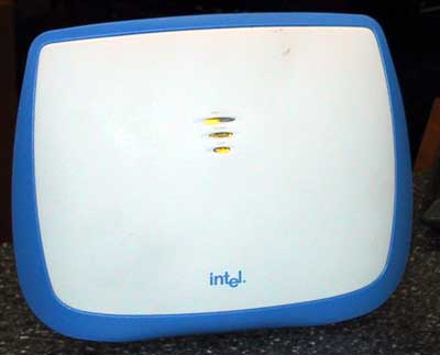
What makes this Internet Gateway any different from your conventional Cable/DSL router? It is actually recognized as a device by Windows XP because of its UPnP support. The Internet Gateway device will then be able to dynamically open and close ports depending on application requests instead of requiring you to do so manually. Of course you’re able to limit how freely the gateway will behave but this is the first step in making dealing with file transfers and video conferencing much easier to use from behind routers.

There are security issues to be worried about but as with all innovations in technology that simplify things, they will be worked out as well as worked around.
Ending on Itanium
Since this isn’t a normal article we can’t really have a normal conclusion, so we thought we’d end on some discussion regarding Itanium and its future. Recently there have been stories hypothesizing Intel dropping Itanium and IA-64 because of the platform’s lackluster adoption and niche market stance. The fact of the matter is that the IA-64 architecture was aimed at a niche market from the start. To put it in Intel’s own words, Itanium was necessary for Intel to design the next-generation of microprocessors. You won’t find Itanium or IA-64 used in the majority of server farms, nor will you find it in most high-end workstations; IA-64 will be reserved for the most demanding of high-end tasks and by definition will be aimed at a very niche market. The 16-way (and beyond) server market makes a lot of sense for Itanium and IA-64, and it is those markets that are predominantly Sun based that Intel is going after.
AMD on the other hand is taking a completely different approach with their x86-64 technology that’s going into Hammer. Although the Hammer architecture will be made ready for extremely parallel MP systems, it won’t be going after the same market as IA-64. Instead, x86-64 will be targeted at the majority of the high-end workstation and server market eventually trickling down to the mainstream. In contrast, the technology and architecture behind Itanium won’t be headed for the mainstream desktop sector anytime soon. Although some of the design innovations that made it into Itanium and future IA-64 CPUs will be used in the desktop sector, it’s unlikely that you’ll see EPIC there anytime soon.
Note that this still doesn’t eliminate the possibility of Intel working on another 64-bit project that would end up competing with AMD’s x86-64 line. If you only take away one thing from this article it should be that above all, Intel is driven by engineering and technology and not by marketing (although it may not always seem that way). If going down an alternate route for bringing 64-bit processing to the mainstream makes sense, you can bet Intel will do it.

You see a lot of familiar names walking around downtown Portland
Until next time
We’ve been talking about doing this type of an article for months now and with it finally completed we’re hoping to do many more like it. In-depth features on what goes on behind companies like AMD and Intel, ATI and NVIDIA.
Let us know what you’d like to see and we’ll try to make it happen.


