Introduction
Founded in 1986, MSI has a long and successful history in the computer component business. They are a top 5 motherboard manufacturer and for the last four years they have held the number one manufacturer position in discrete video card sales. MSI is also an emerging player in the consumer electronics market while also providing a broad range of products from optical drives to wireless network components.
The MSI K8N Diamond Plus motherboard we are reviewing today is the latest board in the Diamond series and offers an excellent feature set and performance level for the AMD enthusiast or gamer. You can find more information about the entire line of MSI products at their website.
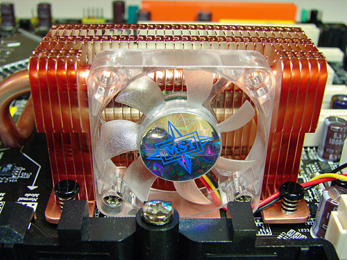
Our initial impression of the MSI K8N Diamond Plus upon opening the box is that it has an extensive feature list, cluttered yet clean layout, heat-pipe cooling system, and that the overall quality of components utilized by MSI is very good. The board retails in the US $190 range and arrives with an extensive accessory and documentation package. Besides the Asus A8N32-SLI and Abit AN8-32X, this is the only other AMD Socket 939 board to feature the NVIDIA nForce4 SLI X16 chipset configuration.
During our testing and general usage of the MSI K8N Diamond Plus we found the board's stability to be superb and it delivered class leading results in most of our synthetic and game benchmarks. Unfortunately, although the latest 3.0a BIOS release has generally improved the board's stability, overclocking options, and performance, we still incurred issues trying to get our particular sample to overclock in a similar fashion to our nForce4, ULi M1697, or ATI RD580/480 boards.
We met with limited success in the overclocking testing phase. While the board provided very competitive results when utilizing the stock multipliers, we had issues trying to POST near, at, or above a 300HTT setting. We tried numerous settings and various components over the entire test period with the board but just could not reach the 300HTT level and remain stable enough to complete our test suite. In the end, we were resigned to stay around a 285HTT level that left us disappointed as all other aspects of this board's performance are excellent.
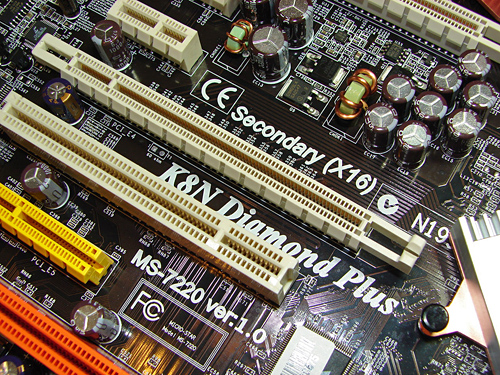
The MSI K8N Diamond Plus offers a complete compliment of options including two physical PCI Express x16 connections (x16 operation in SLI mode), two PCI Express x1 connections, one PCI Express x4, and two 32-bit PCI 2.3 connections. The board also offers HD audio via the Sound Blaster Audigy SE chipset, PCI-E Gigabit Ethernet via the Marvell 88E8053 LAN controller, PCI Gigabit Ethernet via the Marvell 88E1115 PHY, ten USB 2.0 ports (four rear ports and six more available via three USB 2.0 headers), two SATA 3Gb/s connectors via the Silicon Image SiL3132, two ATA133 Ultra-DMA IDE and four SATA 3Gb/s connectors along with IEEE 1394 support from the VIA VT6306 1394A capable chipset.
How is all of this possible? The board is designed around the NVIDIA C51D and nForce4 SLI chipsets that account for a total of 38 PCI Express lanes via 7 independent PCI Express controllers. The C51D chipset acts as the Northbridge and contains 18 PCI Express lanes. Out of these 18 lanes, 16 are consumed for the primary PCI Express x16 graphics slot, one for a PCI Express x1 slot, and the remaining PCI Express lane for the Marvell 88E8053 Gigabit Ethernet controller. The nForce4 SLI chipset acts as the Southbridge and contains 20 PCI Express lanes. 16 lanes are utilized for the secondary PCI Express x16 graphics slot with one lane going to the second PCI Express x1 slot, one for the Silicon Image 3132 SATA controller, and the final two lanes powering the PCI Express x4 slot which limits its actual performance to x2 capability. The VIA VT6306 IEEE 1394, Marvell 88E1115 Ethernet PHY, and Creative Labs Audigy SE chipsets are PCI based with traffic being routed through the Southbridge.
Due to the splitting of the PCI Express lanes between the Northbridge and Southbridge for the x16 graphics capability, plus the various peripheral traffic between the two bridges, and it could be argued this design will limit or hamper performance. Though this design does not consolidate all of the PCI Express lanes for graphics operations into a single chip solution such as the ATI Radeon Xpress 3200 (RD580) chipset, we did not notice any ill effects or slowdowns in our testing. In fact, with a 16-bit 1GHz HyperTransport link providing up to 8GB/s of bandwidth, the bandwidth available between the two bridge chipsets is the same as the bandwidth between the Northbridge and the Socket 939 CPU.
Now let's take a closer look at the features and performance the MSI K8N Diamond Plus offers.
Founded in 1986, MSI has a long and successful history in the computer component business. They are a top 5 motherboard manufacturer and for the last four years they have held the number one manufacturer position in discrete video card sales. MSI is also an emerging player in the consumer electronics market while also providing a broad range of products from optical drives to wireless network components.
The MSI K8N Diamond Plus motherboard we are reviewing today is the latest board in the Diamond series and offers an excellent feature set and performance level for the AMD enthusiast or gamer. You can find more information about the entire line of MSI products at their website.
Our initial impression of the MSI K8N Diamond Plus upon opening the box is that it has an extensive feature list, cluttered yet clean layout, heat-pipe cooling system, and that the overall quality of components utilized by MSI is very good. The board retails in the US $190 range and arrives with an extensive accessory and documentation package. Besides the Asus A8N32-SLI and Abit AN8-32X, this is the only other AMD Socket 939 board to feature the NVIDIA nForce4 SLI X16 chipset configuration.
During our testing and general usage of the MSI K8N Diamond Plus we found the board's stability to be superb and it delivered class leading results in most of our synthetic and game benchmarks. Unfortunately, although the latest 3.0a BIOS release has generally improved the board's stability, overclocking options, and performance, we still incurred issues trying to get our particular sample to overclock in a similar fashion to our nForce4, ULi M1697, or ATI RD580/480 boards.
We met with limited success in the overclocking testing phase. While the board provided very competitive results when utilizing the stock multipliers, we had issues trying to POST near, at, or above a 300HTT setting. We tried numerous settings and various components over the entire test period with the board but just could not reach the 300HTT level and remain stable enough to complete our test suite. In the end, we were resigned to stay around a 285HTT level that left us disappointed as all other aspects of this board's performance are excellent.
The MSI K8N Diamond Plus offers a complete compliment of options including two physical PCI Express x16 connections (x16 operation in SLI mode), two PCI Express x1 connections, one PCI Express x4, and two 32-bit PCI 2.3 connections. The board also offers HD audio via the Sound Blaster Audigy SE chipset, PCI-E Gigabit Ethernet via the Marvell 88E8053 LAN controller, PCI Gigabit Ethernet via the Marvell 88E1115 PHY, ten USB 2.0 ports (four rear ports and six more available via three USB 2.0 headers), two SATA 3Gb/s connectors via the Silicon Image SiL3132, two ATA133 Ultra-DMA IDE and four SATA 3Gb/s connectors along with IEEE 1394 support from the VIA VT6306 1394A capable chipset.
How is all of this possible? The board is designed around the NVIDIA C51D and nForce4 SLI chipsets that account for a total of 38 PCI Express lanes via 7 independent PCI Express controllers. The C51D chipset acts as the Northbridge and contains 18 PCI Express lanes. Out of these 18 lanes, 16 are consumed for the primary PCI Express x16 graphics slot, one for a PCI Express x1 slot, and the remaining PCI Express lane for the Marvell 88E8053 Gigabit Ethernet controller. The nForce4 SLI chipset acts as the Southbridge and contains 20 PCI Express lanes. 16 lanes are utilized for the secondary PCI Express x16 graphics slot with one lane going to the second PCI Express x1 slot, one for the Silicon Image 3132 SATA controller, and the final two lanes powering the PCI Express x4 slot which limits its actual performance to x2 capability. The VIA VT6306 IEEE 1394, Marvell 88E1115 Ethernet PHY, and Creative Labs Audigy SE chipsets are PCI based with traffic being routed through the Southbridge.
Due to the splitting of the PCI Express lanes between the Northbridge and Southbridge for the x16 graphics capability, plus the various peripheral traffic between the two bridges, and it could be argued this design will limit or hamper performance. Though this design does not consolidate all of the PCI Express lanes for graphics operations into a single chip solution such as the ATI Radeon Xpress 3200 (RD580) chipset, we did not notice any ill effects or slowdowns in our testing. In fact, with a 16-bit 1GHz HyperTransport link providing up to 8GB/s of bandwidth, the bandwidth available between the two bridge chipsets is the same as the bandwidth between the Northbridge and the Socket 939 CPU.
Now let's take a closer look at the features and performance the MSI K8N Diamond Plus offers.


42 Comments
View All Comments
OvErHeAtInG - Tuesday, April 18, 2006 - link
Let me be the devil's advocate here. I know AT reviews (and others) usually regard same-colored RAM slots to be "correct" for dual-channel operation, but for me it's always made more sense when it's like this MSI board--one color for each channel. Of course, it wouldn't be confusing if manufacturers just chose one standard color scheme and left it at that.Gary Key - Thursday, April 20, 2006 - link
We completely agree about having a standard color scheme. The majority of boards have different colors for dual channel operation so our comments are based this fact. A previous MSI board we tested followed this pattern and then they change it on this board. It is too confusing in my opinion when a single supplier cannot agree on a color scheme between board releases. This is certainly not an MSI only issue either. :)
Wesleyrpg - Tuesday, April 18, 2006 - link
Hmmm, is this common knowledge? One of my friends suffers from this so badly that we had to set up his cable modem for use the the USB port (yuck). Is there a workaround/beta drivers? I'm sure NVIDIA wouldnt want this leaked if it was true? Why havent they done anything about it? The current AMD driver 6.70 is about 6 months old now and still corrupts data. Damn them!!!!
Gary Key - Thursday, April 20, 2006 - link
Yes, this is fairly common knowledge and we have actually referred readers to NVIDIA for assistance. I do have a new set of drivers for the Business Platform system and will be testing them next week.
Wesleyrpg - Tuesday, April 18, 2006 - link
hmmm, seems NVIDIA have more than just an issue with their ActiveArmor, from what i have been reading theres also huge problems with the IDE/SATA file tranfers as well. Wish i'd know about these issues earlier, up until today i been recommending the NFORCE4, but with all these issues its hard to recommend them at all. Why hasnt any articles been written up on the MAJOR issues with the Nforce4 chipset?Per Hansson - Sunday, April 16, 2006 - link
Just replying to your message to me in the other mobo review "Please email me - I have the photographs. We are doing some revisions on the engine and could not get these in but I did take the photographs for you."I'm not the one that needs the pictures, I can identify the caps anyway... I was just thinking that it would be a nice addition to your articles, incase there where other readers that where interested in this too...
This board looks really nice though, United Chemicon KZG everywhere it seems, except for the Sanyo Polymers at the VRM and plenty more than what should "really" be necessary for a budget board like this... (okay, there looks to be one or four odd caps in the PCI section but they do oftenly not see very much ripple current so it should be ok)
tekkstore - Monday, April 17, 2006 - link
http://www.tekkstore.com">tekkstore.comAnnonymousCoward - Friday, April 14, 2006 - link
Macs still don't have a right mouse button? When will they put their stubbornness behind?goinginstyle - Wednesday, April 12, 2006 - link
I think you guys need to check your facts on the southbridge. According to the HardOCP article the board has the ULi 1575 southbridge. Are you sure the board has the nforce4 sli on the southbridge as that chipset is usually on the northbridge .Gary Key - Wednesday, April 12, 2006 - link
We will not comment in an open forum about another website's information that might or might not have been posted. However, I can ensure you this board utilizes the NVIDIA nForce4 SLI for the Southbridge (MCP) and the C51D for the Northbridge (SPP) as explained on the front page. If you still question our statements, then please visit MSI's website where the chipset information is available for this board - http://www.msi.com.tw/program/products/mainboard/m...">MSI K8N DiamondThanks!