Globalfoundries Starts on 22nm Fab & Announces First non-AMD Customer
by Anand Lal Shimpi on July 29, 2009 4:01 AM EST- Posted in
- CPUs
Somehow I’d managed to dodge meeting with Globalfoundries since the company was formed earlier this year. For those of you who don’t know, AMD is now officially a fabless semiconductor. AMD provided its two existing fabs to the new company and its partner, ATIC (Advanced Technology Investment Company) provided $6B. ATIC owns 65.8% of the new company and AMD owns the rest, although the two share voting rights.
AMD’s biggest limitation has always been capital. Intel currently has four fabs that will be producing 32nm chips by the end of 2010, AMD currently has (err, had) a single 45nm fab in Dresden. There’s simply no way AMD could compete in the fab game with Intel, so it chose to partner up with ATIC, take $6B of their dollars, and spin off its fab business.
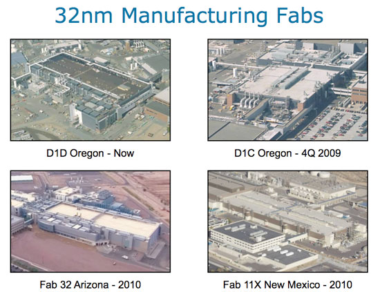
Intel's 32nm fabs for 2010
Until this morning, Globalfoundries only had a single customer - AMD, but that just changed with the announcement that STMicro would be using their fabs. Currently Globalfoundries only has AMD’s two fabs in Dresden, Germany, only one of which is producing modern 45nm SOI wafers. But that too is about to change.
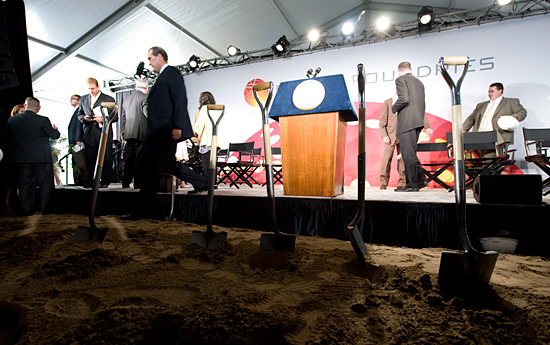
Ceremonial shovels, at a ceremonial ground breaking
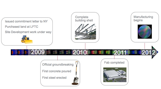
My first official meeting with GF came just this past week, in Saratoga County, NY. That’s the site where its brand new post-AMD fab will be constructed and it’s sort of a big deal. I was there for the ceremonial ground breaking, but concrete doesn’t get poured until September, the shell won’t be finished until 2010 and the fab won’t be done until 2011. Globalfoundries won’t be able to ship revenue generating wafers until 2012. But that’s ok, with $6B in the bank and a strong commitment from wealthy ATIC the company couldn’t be in a better place.
On Competing with TSMC
AMD couldn’t last competing in the foundry game with Intel. The chart below just shows how expensive it gets:
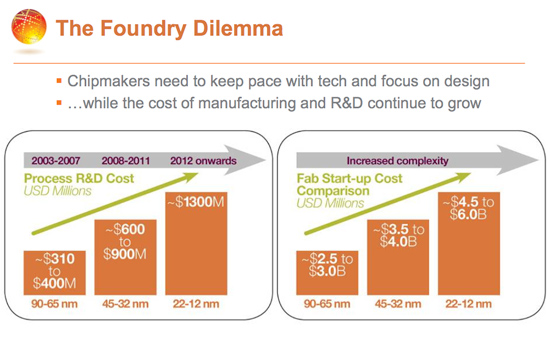
At 32nm a single fab can cost $4B and in just two years it’ll need to be upgraded (to the tune of around a billion) to support 22nm production. For AMD to support the costs alone and remain competitive with Intel, it would have to virtually own the x86 microprocessor market. Even when AMD held the technology crown, that didn’t happen.
The other alternative is to subsidize the cost of these expensive factories over multiple customers. This is where things get interesting. AMD alone may not be able to fill a fab and make the investment pay off, but AMD + Sony + Toshiba + NVIDIA + etc... can definitely make it work.
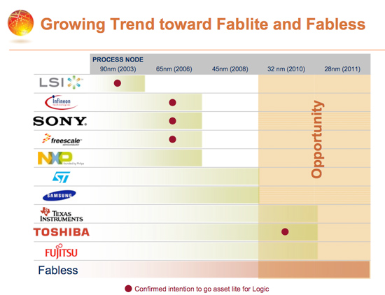
Globalfoundries' potential customers and when they plan on going fabless
Currently, fabless semiconductor manufacturers like NVIDIA (and the graphics division of AMD) go to foundry companies like TSMC for their manufacturing needs. In return, they get nearly the latest manufacturing processes (TSMC is at 55nm for volume and 40nm while Intel is at 45nm moving to 32nm) and don’t have to worry about building expensive fabs.
There are problems with this approach. For starters, TSMC has been having troubles moving to 40nm - as you may have heard. Just as important, you don’t get the most advanced manufacturing process technically available. There’s also the fact that TSMC has very little real competition in the industry; all of the GPUs you’re used to reading about are made at TSMC.
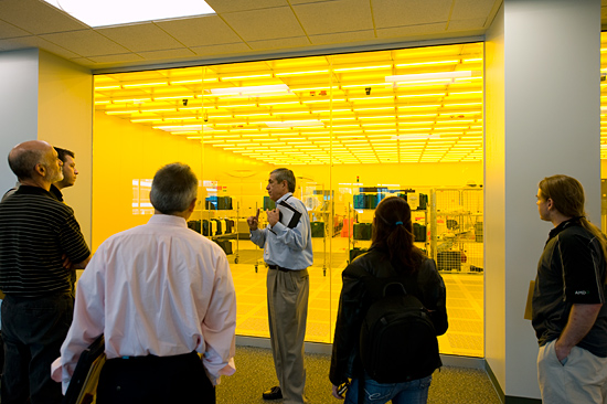
The machine to the left of the man's head in the center of the pic is a 193nm lithography machine. We weren't allowed to take close photos, but that machine costs around $75M. Fabs are expensive.
Companies like Sony, Freescale, Samsung, Toshiba and TI all currently fab their own chips. These chips are far less complex than a Nehalem or a Radeon HD 4890 and are thus made on 130nm, 90nm or 65nm processes. The SoC (System on Chip) in the iPhone 3GS is built on a 65nm process by Samsung at its own fab. Being able to move to 45nm or 32nm alongside Intel would give Apple, Samsung and even ARM in general a tremendous competitive boost in the market place. A 45nm iPhone 3GS would use less power or even run at higher clock speeds.
The need for a modern fab partner increases as you look at Intel’s motions towards competing in the smartphone space. Once Atom finally makes its way into smartphones, Intel could have a manufacturing advantage over the ARM partners - allowing for quicker scaling to lower power and higher performance designs. In other words, companies making smartphone SoCs need a good foundry option to compete with Intel.


50 Comments
View All Comments
drwho9437 - Saturday, August 8, 2009 - link
I think Anand is correct that FABs are ridiculously expensive and that the volume leader has a major advantage. However, it remains to be seen if the spin off is a good move for AMD.The honest truth is that 15 nm is probably the end of the road for gate lengths. That is a few generations away. Lithography can improve all you want it to, but leakage and process variability become more and more important as you go down in size. At 10 nm cube of Silicon has about 100,000 atoms in it. Even at 10^20 /cm^3 doping levels you are talking about 100 atoms in the channel. That's 10% variability in doping... 32 28 22 18 end of the road my friends. Of traditional Silicon that is. There really isn't anything right now to easily replace it, its just so nice chemically...
People will say the end has been predicted forever, and then claim I am wrong (at least that is what normally happens when I say this). I may be wrong but that isn't why. The sun comes up every day but one day it won't. One day we will hit the physical limits of Silicon and from my point of view it will be the statistical that will certainly be a problem. I think you'll see problems at around 10-15 nm.
What is exciting it the idea that we will have to finally be more cleaver than drawing smaller lines in Si and think of something truly original to make progress...
But given that that original idea may either take time to materialize or that it might be expensive, I think you will see reliable Si for a LONG time at some dimension. 40 or 32 nm may be with us a for decades in many types of systems... Given this, the cost of upgrading FABs may stop because there will be no more upgrades. Then you ask do you want control over them or not... I can see arguments on both sides. Certainly in the near future AMD had no choice cash flow wise.
There are other ways to innovate other than die shrinks, and leaning on optics and chemistry. We shall see if we are cleaver enough.
cosminliteanu - Monday, August 3, 2009 - link
Thank you for this article :)zodiacfml - Sunday, August 2, 2009 - link
Thanks Anand! Some good posted comments too.toyotabedzrock - Saturday, August 1, 2009 - link
$88M / 1,400 Jobs = $62,875. So a lot of the jobs must be for not highly skilled people? I consider highly skilled to be worth $80-100K.Doesn't the US control how much of our most advanced tech is exported to certain countries? We only just recently allowed Intel to build a 65nm fab in China.
drwho9437 - Saturday, August 8, 2009 - link
Typical FAB worker would probably hold a BS in EE, Chem, Mat Sci, starts at about 42-50K when I graduated undergrad. Those 10K slots add up for the MS/PhD who run the line or whatever.mesiah - Thursday, July 30, 2009 - link
Great article! I love reading stuff like this. I am by far not an expert in the field, but it sounds like EUV could revolutionize the chip making process. Although it looks like it still has a significant number of hurdles to overcome, especially when it comes to WPH. Also an exciting prospect but many more years off is the current research with graphene. Its hard to imagine the processing power we will be able to harness in the near future. Alot of people take for granted the devices we use today. Things like iphones and netbooks were hardly dreamed of when I was a kid. Sure, we talked about seeing stuff like this 15 years ago, but I guess I never believed it would happen so fast.MODEL3 - Wednesday, July 29, 2009 - link
Great article.I just have some questions regarding fab companies such TSMC:
Until 180nm, we had a very good tempo for manufacturing proccess transitions.
Then suddenly, from 180nm to 90nm there was a very profound deceleration.
Then from 90nm to 40nm (and for the medium-term future) we have an increase of the tempo again.
Why they keep increasing the tempo?
You said that the R&D cost increased dramatically and that the Fab Start-up Cost increased dramatically also. (I am not arguing, after all I don't have a technological background)
So if for a company such TSMC, the cost has increased so much more in relation with the past then it should charge their customers per wafers (per size counted in) much more, right?
Then Why between 90nm and 55nm:
The die size per price range increased exponentially (I have done the calculations with Nvidia chips because the "die information" was more easily found on the net)
This is a fact.
Unless that your explanation is simply that Nvidia & ATI made way way more money back then, or that TSMC was robbing Nvidia/ATI back then, what is your explanation?
I mean that, yes it is easy to figure out that Nvidia & ATI made more money back then, but the financial data does not support such a huge difference.
My guess (out of the conspiracy book) is that already exists a valid successor of silicon based type methods and they just milking the current technology (for the next 5-10 years)
(I am not talking about technologies to scale down lithography, like alpha EUV, I am talking about THE next step to silicon based types)
In another subject you said:
Note that this 28nm process is a “half-node” (between 32nm and 22nm) and where I’m expecting to see ATI (and NVIDIA) GPUs made at Globalfoundries"
Why are you expecting 28nm to be that process?
Do you think that after 28nm the TSMC will skip 22nm (like they did with 45nm) and focus on 20nm (so the transition will take them more time), so GF will find an opportunity to offer something competitive?
drwho9437 - Saturday, August 8, 2009 - link
High K and SOI both expensive gave new breathing room. But they both are stop gap measures... Bigger problems to come. Expect 32 nm and the next node to go OK then bigger fish enter the picture.Also don't expect way higher frequencies. 2 GHz is pretty easy to design. I can do a PCB that is flat to 2 GHz in about an hour... Designing in the X band however is painful.
Still all sorts of interesting things going on outside Si, organics, molecular switches, terahertz, optics on chips, the return of magnetic. They are all pain in the butt compared to better lithography though :-)
Zagor Tenay - Wednesday, July 29, 2009 - link
Great article! It is so relieving to see that the whole semiconductor industry is not a captive at the hands of an ugly, greedy beast called INTEL.Zingam - Wednesday, July 29, 2009 - link
Don't forget that AMD owns the GF. If GF makes a profit. AMD gets revenues.I don't think that AMD does not have foundries anymore. They are just not attached to it. It isn't the same as NVIDIA - they do not possess anything like GF.