Intel's Atom Architecture: The Journey Begins
by Anand Lal Shimpi on April 2, 2008 12:05 AM EST- Posted in
- CPUs
2-Issue and In-Order: Intel's Version of the Cell's PPE
The Austin design team started with a single-issue in-order core but quickly expanded it to be a superscalar, 2-issue design, in other words it is capable of sending up to two instructions down the pipeline at the same time. By comparison most desktop x86 microprocessors are 3 or 4-issue designs.
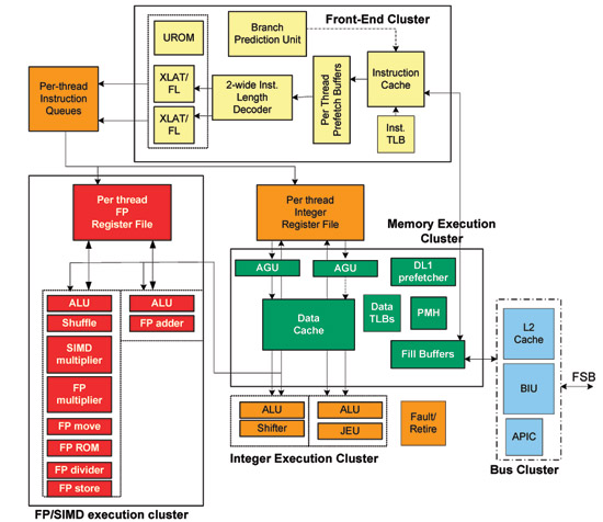
In order to feed the 2-issue machine, Intel equipped Atom with two decoders. These decoders take instructions fetched from the L1 instruction cache and sequence the series of 1s and 0s into figuring out what the instructions are telling the CPU to do. While the decoders are equal in their ability to decode instructions, there are two paths that an instruction may take: slow and fast.
In the earlier days of the x86 ISA (Instruction Set Architecture) many complained about its support for variable length instructions.
If I tell you that I'm going to give you 2 oranges every 10 seconds, your job becomes much easier than if I tell you that I'm going to give you somewhere between 1 and 3 oranges every 10 seconds. The former would be an example of a fixed length instruction set and the latter a variable length instruction set, unfortunately x86 falls into the realm of the latter.
Atom's slow decoding path does not include any speculative decoding. The instructions are sequenced manually, meaning that each bit is looked at (which takes time) but the instruction is guaranteed to be decoded properly. The instruction is also tagged so that the next time it comes through it can be sent through the fast path.
The fast path obviously employs some speculative decoding and is aided by the tag bit that's set after an instruction goes through the slow path. The slow path yields 1 instruction every 3 clocks, while the fast path can produce 2 instructions every clock.
As Intel learned with Banias (Pentium M), the power penalty for incorrect speculation is unacceptable in a device running on a battery. You'll see a number of tradeoffs where speculative performance tricks are sacrificed in order to maintain low power operation with the Atom processor.


46 Comments
View All Comments
adntaylor - Tuesday, April 8, 2008 - link
On that chart with price / power, you need to be clearer...For price, you show the combined price for CPU + Chipset. For power, you say just the CPU... so 0.65W for the CPU... but you're conveniently ignoring the >2W figure for the chipset!!! This absolutely flatters Intel wherever possible.
AMD are just as misleading - they describe the Geode LX as "1W" which excludes the non-CPU core parts of the chip (which is an integrated CPU + GMCH)
Just please be honest - the figures are out there in the Intel datasheets... it takes 10 minutes to check.
Clauzii - Friday, April 4, 2008 - link
I still have a PowerVR 4MB addon card, runnung in tandem with a Rage128Pro. Quite a combination w. 15 FPS in Tombraider. Constant(!) 15FPS, that is..Amazing what they actually achieved back in 95!
Clauzii - Friday, April 4, 2008 - link
Ooops!Totally misplaced that. Sorry.
wimaxltepro - Friday, April 4, 2008 - link
The Atom represents a shift in processor architecture that is the most dramatic departure for Intel since introduction of x86 processors... the philosophy of how computing itself occurs from centralized processors to distributed processing based on an extension of the popular x86 instruction set.The Atom is not about the immediate prospects for the Atom or Nehalem products: we will likely see members of Intel's new product family be used in embedded applications in consumer products and in areas where specialized communications processors are more the rule. While not optimized for use in specific networking applications, the products capitalize on the wide range of support available in IT/Networking to develop common functions that leverage the low cost, low power/processing capability to be used as a common denominator for a wide range of applications.
Intel has been built on the 'Wintel' architecture: massively integrated chips needed to handle the massively integrated operating systems and applications of Windows (and Apple) environments. The Atom allows migration and broadening out from that architectural motif to a very highly distributed architecture. So, the increased parallelism found in the internal chip architecture is enabling of changes in external system architectures and device applications that go well beyond the typical domain of Intel.. and right into the domain of 'personal wireless broadband' and SDWN, Smart Distributed Wireless broadband Network.
The decisions about in-order vs. out of-order instruction streams, memory architecture, I/O architecture have been made in light of the broad vision for how computing, networking and, out of hand, how wireless enabled broadband networking including WiMAX will occur. This should be understood for what it represents as a shift in direction for Intel both in response to broad industry shifts and as a trend setting development.
jtleon - Friday, April 4, 2008 - link
Thanks to all the flash player ads, etc., a mobile web device will continuously avoid switching to low power states. Thus one could argue that advertising will be carbon footprint enemy of the internet's future. This is already becoming the case for desktop/laptop machines.Without such continuous (arguably wasted) consumption of CPU power, then Intel's engineered power management might have a significant impact on the value of the Atom.
Regards,
jtleon
0WaxMan0 - Friday, April 4, 2008 - link
I am definatly much impressed and enthused by intels work here, the future looks interesting esp for those of us who like low power cross compatible computing products.However I have to point out that a low power modern x86 cpu has allready been done infact 4 years ago with AMD's Geode. While technically much weaker than the Atom and with out any where near the scalability (single core design etc.) the Geode has been available in the same TDP ranges for a good long while. Take a look here http://www.amdboard.com/geode.html">http://www.amdboard.com/geode.html for some old stuff.
I do hope that the Intel name and hype makes more of an impact than AMD managed.
whycode - Thursday, April 3, 2008 - link
Does the TDP quoted include the chipset? Or is that CPU only?IntelUser2000 - Thursday, April 3, 2008 - link
Anand, the Pentium M does not feature Macro Ops Fusion. Its Core 2 Duo that started Macro Ops Fusion.Anand Lal Shimpi - Thursday, April 3, 2008 - link
You're correct, I was referencing micro-op fusion. I've made the appropriate correction :)Take care,
Anand
squito - Wednesday, April 2, 2008 - link
Am I the only one shocked to see that Poulsbo is a 130nm part...