AMD's Next-Generation Mobile Architecture Revealed: Griffin
by Anand Lal Shimpi on May 18, 2007 12:10 AM EST- Posted in
- CPUs
Platform
Just like Intel bundles its mobile CPUs and chipsets as platforms, AMD is doing the same with Griffin. Puma is the name of Griffin's launch platform, but unlike Intel's approach the platform only consists of a Griffin CPU and an AMD chipset; wireless networking is provided by any number of third party vendors. The CPU we already know about, but the chipset is AMD's upcoming RS780.
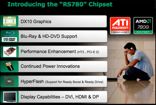
The chipset supports Hyper Transport 3 (obviously), PCI Express 2.0 (faster link speeds/higher bandwidth) and AMD's answer to Intel's Turbo Memory, Hyper Flash.
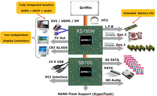
The RS780 features an integrated graphics core based on the R600 architecture, however AMD would not provide us any details at this point in time other the following two points. The integrated GPU will feature H.264 decode acceleration, which we're assuming is the same full pipeline UVD from the desktop R600.
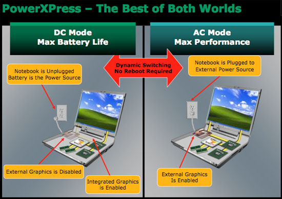
Even more interesting is the platform's support for a feature called PowerXPress. The idea is that all Puma notebooks will have integrated graphics, but they can also have optional discrete graphics for better gaming performance. AMD is confident that its integrated graphics will be lower power than any discrete graphics solution, so when you're running on battery power the external graphics core would be disabled and your display would run off of the integrated GPU. On AC power, in the max performance mode, the internal graphics gets disabled and the external GPU is operational.
According to AMD, this switchover happens seamlessly; there's no reboot required and there should be hardly any interruption in use. We have yet to see it in action and are understandably skeptical of how smooth the transition between GPUs would be, but AMD claims that it works and very well at that. AMD also mentioned that this functionality could be overridden by a control panel if need be.
Griffin will use the same S1 CPU socket as current Turion CPUs, however the pinout will be different meaning that these new chips won't be backwards compatible with current Turion notebooks.
As we mentioned above, Hyper Flash will be supported by the RS780 chipset but not over the PCI Express bus. Instead, AMD is using a proprietary interface between the South Bridge and its Hyper Flash controller. According to AMD, PCI Express is not the most power efficient interface to NAND flash so it is using an alternative. AMD expects performance of Hyper Flash to be noticeably better than Intel's Turbo Memory, but without numbers to put to that claim we can't think much of it (it's rare that a manufacturer makes claims about how slow its technology is going to be).


36 Comments
View All Comments
Roy2001 - Friday, May 18, 2007 - link
AMD stated that it didn't want to clue Intel in on what it had up its proverbial sleeve----------------------------------------------------------------
I really want to laugh. 64bit is really a revolution? What else AMD invented except IMC? Intel invented X86 and AMD copied it.
TA152H - Friday, May 18, 2007 - link
AMD invented the integrated memory controller? You're joking, right?They weren't even the first x86 company to make one, it was NexGen, a company they bought when they realized they weren't competent enough to make their own x86 processors without copying Intel. It was during the K5 debacle, and Jerry Sanders was smart enough to buy them, and that is where the K6 came from.
AMD copied a lot more than x86 from Intel. I actually have one of their 1981 product sheets, they even copied Zilog stuff like the Z8001 and Z8002. They, of course, copied the 8080 and 8085 as well. So, the fellow that goes on about IBM making that relationship is dead wrong. It started a lot sooner than that, and only when Intel got greedy with the 386 was it ended with acrimony. Intel was annoyed AMD would sell everything for so cheap.
Regs - Sunday, May 20, 2007 - link
Thank god for the caveman that invented the wheel or we really be screwed.Do you guys get hard-on's googling information about who "invented" what first just to shove it back at someone's face? Who knows, maybe the guy who invented the IMC now works for AMD. Who the hell knows what original idea or concept it came from either. Though I'd say AMD did a hell of a job making it work!
TA152H - Sunday, May 20, 2007 - link
What a dork.You think I used Google for this? You wouldn't understand because you're a moron, but it bothers me when people say things I know are wrong and perpetuate misinformation.
They had built computers on a chip well before the x86 world ever saw the IMC, so making weird claims about AMD and them inventing the IMC is flat wrong. They were the first to make that tradeoff, but anyone could have done it.
Making it work isn't particularly difficult, and I'm not even sure it's proven to be a great idea. You give up a lot to get it, and only when compared to the ultra-sophisticated, and horrible Pentium 4 did it shine. Against the Core 2, this great feature is part of a product that gets totally raped by Intel's solution. So, I'm not sure it was greatest thing in the world to spend the transistors on, Intel obviously found better ways. Even now, the Barcelona still won't have memory disambiguation like the Core 2, and will have only the store/load OOP ability of the P6 core. It's a step in the right direction, but I'm thinking they should have spent a few more transistors there, although I think they'd be better off taking them from x87. What is the point of that now?
Starglider - Friday, May 18, 2007 - link
AMD copied x86 at Intel's request. Intel was bidding for IBM's original PC project, IBM said 'you must have a second manufacturing source', so Intel contacted AMD, asked them to manufacture 8086 chips and supplied them with the semiconductor masks to do so. AMD cunningly made the ability to use the x86 ISA in their later chips a requirement of the contract, though it took a court case to confirm the legality of this. But no, AMD did not slavishly clone Intel's ISA, Intel specifically asked them to do so.hechacker1 - Friday, May 18, 2007 - link
AMD's announcement sounds like a good idea. It will allow them to catch up to current battery life improving technologies.My Dell 700m inpirion (which costed $800 shipped new 2 years ago) features a pentium-m dothan 1.7GHz single core. Hardly the latest technology. I've managed to get 5+ hours with wifi always on and moderate screen brightness (this screen gets too bright!) in linux.
In windows xp battery life is ~3.9hours with similar usage. In vista it dwindles even further. (note i have 2GB of ram to prevent swap usage/hard disk activity).
But in linux there are great power management capabilities and intel provides a good amount of open source drivers. And now they released this very useful application:
http://www.linuxpowertop.org">http://www.linuxpowertop.org
Already there are many new patches to even further reduce power consumption by badly coded programs. Some of these fixes will work their way into Windows (like firefox), but I wonder how carefully Microsoft evaluated their power consumption due to code?
All of these "extra lower power states" are useless if the software never allows the CPU to reach those lower power states. My own computer had several problems that forced my lowest power state to "C2". After using powertop I have managed to get my computer go into C4 power state. I'll be getting even better battery life now!
As far as AMD is concerned, I believe they have waited too long to match intels capabilities in the fastest growing mobile market. Why wait for Griffen when Santa Rosa is essentially the same? And I already know intel has great open source support (all of my cheap dell hardware works perfectly).
TA152H - Friday, May 18, 2007 - link
How is what is being done with the Barcelona and this Griffin different from what AMD did with the CXT core in the K6-2? They called it write combining back then. It seems remarkably similar to me, but I might be missing something. Can someone elaborate on the differences?tayhimself - Friday, May 18, 2007 - link
AFAICT it is the same thing except one layer down the memory hierarchy. Instead of your (L2) cache controller combining writes to your memory controller, your memory controller combines writes to the memory banks.TA152H - Friday, May 18, 2007 - link
I thought the same thing, but wanted to make sure.One little thing, it was the L1 cache controller, the K6-2 didn't have a L2 cache on the chip, it was on the motherboard. The K6-III, K6-2+, and K6-III+ all had the on-chip L2 cache.
TA152H - Friday, May 18, 2007 - link
OK, this line "while the K8 is arguably a better starting point for a mobile-specific architecture than the P6", is completely wrong, even though it is qualified.Are you kidding? Do you remember the K7 when it came out and how it compared to the Pentium III? Sure it was faster, but the power use was WAY higher and in no way consistent with the marginal performance improvement. Once you improved the cache on the Pentium III with the Coppermine, and did so later with the Thunderbird, the difference in performance was greatly reduced. People were still preferring the Tualatin 1.4 to the newer stuff until the Core 2 came out, because they were so power efficient and easy to cool, and the performance was excellent, mainly because of the 512K cache. The main reason the Athlon had any advantage, which it did because of frequency headroom is the Pentium III was seriously memory bottlenecked, and that wasn't a huge architecture step forward.
More to the point, why didn't they start with the K6-III????? It was way better than the Pentium III in terms of performance per watt, although not so in floating point. But, AMD is always talking about these coprocessors, so put a K6-III that is cleaned up a little to address its deficiencies, integrate the northbridge and graphics into it (it's a tiny die, it would still be small) and put a small socket for a coprocessor if people need floating point. Why put a power hog like the K8 as the starting point? They could also make a K8 mobile part for the devil may care about power mobile group, but I think the K6 derived group would have extremely low power use, function very well, and be relatively inexpensive to make. A K6-III+ at 600 MHz, even with terrible memory bandwidth and a tiny 256K L2 cache still does fine surfing the internet and opening office apps, etc... Someone needs to go back to these shorter pipelined units for power savings, I was hoping it was AMD. Intel doesn't really have anything, the Pentium wasn't decoupled, and the Pentium Pro had the long pipeline :( .