The Era of Tera: Intel Reveals more about 80-core CPU
by Anand Lal Shimpi on February 11, 2007 5:44 PM EST- Posted in
- CPUs
With no Spring Intel Developer Forum happening this year in the US, we turn to the International Solid-State Circuits Conference (ISSCC) for an update on Intel's ongoing R&D projects. Normally we'd hear about these sorts of research projects on the final day of IDF, these days presented by Justin Rattner, but this year things are a bit different. The main topic at hand today is one of Intel's Tera-scale computing projects, but before we get to the chip in particular we should revisit the pieces of the puzzle that led us here to begin with.
Recapping Tera-Problems
At the Spring 2005 Intel Developer Forum, Justin Rattner outlined a very serious problem for multi-core chips of the future: memory bandwidth. We're already seeing these problems today, as x86 single, dual and quad core CPUs currently all have the same amount of memory bandwidth. The problem becomes even more severe when you have 8, 16, 32 and more cores on a single chip.
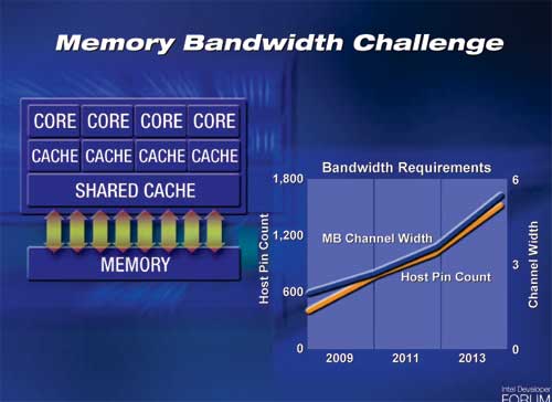
The obvious solution to this problem is to use wider front side and memory buses that run at higher frequencies, but that solution is only temporary. Intel's slide above shows that a 6-channel memory controller would require approximately 1800 pins, and at that point you get into serious routing and packaging constraints. Simply widening the memory bus and relying on faster memory to keep up with the scaling of cores on CPUs isn't sufficient for the future of microprocessors.
So what do you do when a CPU's access to data gets slower and more constrained? You introduce another level in the memory hierarchy of course. Each level of the memory hierarchy (register file, L1/L2/L3 cache, main memory, hard disk) is designed to help mask the latency of accessing data at the level immediately below it. The clear solution to keeping massively multi-core systems fed with data then is to simply put more memory on die, maybe an L4 cache perhaps?
The issue you run into here is that CPU die space is expensive, and the amount of memory we'd need to keep tens of cores fed is more than a few megabytes of cache can provide. Instead of making the CPU die wider, Intel proposed to stack multiple die on top of each other. A CPU die, composed of many cores, would simply be one layer in a chip that has integrated DRAM or Flash or both. Since the per-die area doesn't increase, the number of defects don't go up per die.
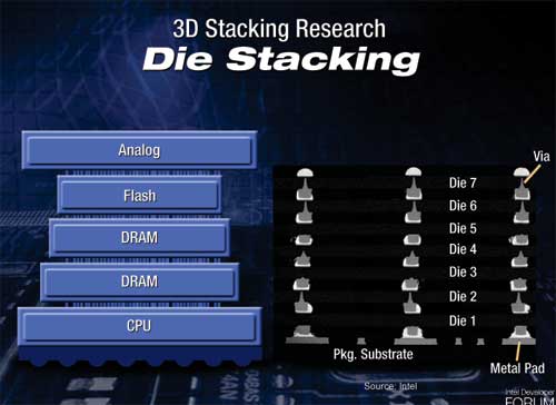
Memory bandwidth improves tremendously, as your DRAM die can have an extremely wide bus to connect directly to your CPU cores. Latency is also much improved as the CPU doesn't have to leave the package to get data stored in any of the memory layers.
Obviously there will still be a need for main memory, as Intel is currently estimating that a single layer could house 256MB of memory. With a handful of layers, and a reasonably wide external memory bus, keeping a CPU with tens of cores fed with data now enters the realm of possibility.
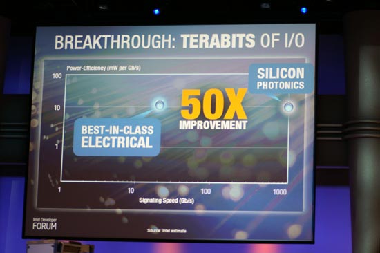
A year and a half later, Rattner was back but this time he was tackling another aspect of the era of tera - bus bandwidth. Although 3D die stacking will help keep many cores on a single die fed with data, the CPU still needs to communicate with the outside world. FSB technology, especially from Intel, has remained relatively stagnant over the past several years. If we're talking about building CPUs with tens of cores, not only will they need tons of memory bandwidth but they'll also need a very fast connection to the outside world.
Intel's research into Silicon Photonics has produced a functional hybrid silicon laser demonstrated at the Intel Developer Forum late last year. The idea is that optical buses can offer much better signaling speed and power efficiency than their electrical equivalents, resulting in the ideal bus for future massively multi-core CPUs.
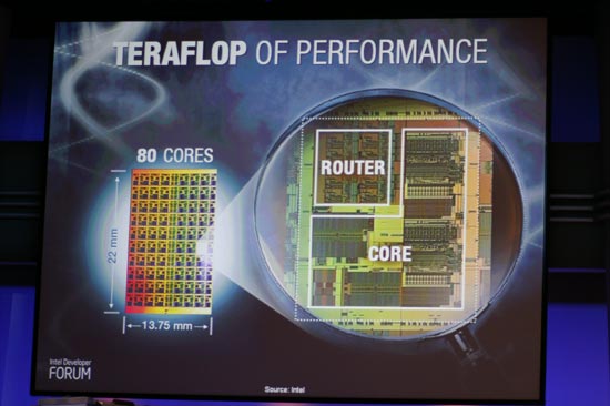
Justin Rattner's keynotes talked about some of Intel's Tera-scale projects, with 3D die stacking delivering terabytes of bandwidth needed for the next decade of CPUs and silicon photonics enabling terabits of I/O for connecting these CPUs to the rest of the system. The final vector that Rattner spoke about, was delivering a teraflop of performance. The CPU Rattner spoke of was a custom design by Intel that featured 80 cores on a single die, and today Intel revealed a lot more about its Teraflop CPU, the architecture behind it and where it fits in with the future of Intel CPUs.


25 Comments
View All Comments
F1N3ST - Monday, February 19, 2007 - link
800 cores for 10 TFlops I say.jiulemoigt - Wednesday, February 14, 2007 - link
maybe 80 un-synced in-order chips is pointless but that stack as a mem controller80 socketed un-synced in-order chips is pointless, since most of the functionally comes from branch logic and out-of-order operations, and not syncing them together means that you could not pass data through them only to them, and even then, issues with passing data would be a mess.
Yet that stack sitting underneath a modern cpu, especially if it could be used as a modern memory stack, with cache speed data access to four cores, that would speed many corp customers could use. Though the memory controller on the chip in the center to control the data flow treat the system memory as virtual extension of it, just like modern hard drives are virtual extensions of system memory, now we are a talking about access data as fast as we can use it. Though the branch logic is going to have to get even better.
najames - Monday, February 12, 2007 - link
Remember the Itanimum and the BILLIONS of dollars Intel spent on the thing? Remember how they thought every company would buy them by the truckload? Remember how expensive they were?Intel did deliver on the Core 2, but I am still leary of anything they hype up.
Brian23 - Monday, February 12, 2007 - link
I know that this chip won't run x86 code, but how does a Core 2 Duo 6600 compare to this as far as teraflops go?AnnihilatorX - Monday, February 12, 2007 - link
I believe that due to physical structures of the silicon lattice silicon is just not a good material candidate for a silicon-on-chip design. Exact same reason why blue laser diodes are made of Gallium arsenide rather than silicon.It's time to move on the much faster and better material than silicon.
fitten - Monday, February 12, 2007 - link
Yes, but silicon has the advantage of beinga) very cheap, comparatively
b) plentiful
benx - Monday, February 12, 2007 - link
I think it is time to stop building computers around the van neumann cycle idea. There wil always be the FSB preformance hit. To counter the problem cpu builders just add more L1/L2/L3 and now maybe L4?time to make the intel cycle with out fsb =)
fikimiki - Monday, February 12, 2007 - link
80 cores sounds great for webserver, java or paralell-processing but how does it stand against to the price and performance of 4 x QuadCore stacked on a single board?Intel is trying to achieve the same thing as Transmeta or just show the marketing muscle once again. I'm sure that Teraflop is going to loose with specialized variety of chips like nVidia, ATI, Cell or Opteron together. You put 3-4 of those and that's it.
We hear that R580 (ATI) can run some calculations 20x faster than ordinary x86, the same with Cell so what the hell is teraflop chip? Especially with integer only calculations?
JarredWalton - Monday, February 12, 2007 - link
I think you're missing the point of this article and the processor. Intel has no intention of ever releasing this particular Teraflop chip into the mainstream market. This is an R&D project, nothing more nothing less. All you have to do is look at the transistor counts to realize that performance isn't going to be competitive right now. Intel chose 80 cores simply because that was what fit within their die size constraints. If they could've fit 100 cores, they would have done that instead.In the future, Intel is going to take some of what they've learned with this research project and apply it to other processors that they actually intend to mass produce and sell. That probably won't happen for several more years at least, and when they get around to releasing those chips you can be sure that they won't have 80 cores and that the course of that they do have won't be anything like the simple processing units on this proof of concept.
How long before anything like this ever becomes practical on desktop computers? How long before it becomes necessary? Those are both interesting questions, and software are obviously has a long way to go first. I have no doubt that someday people are going to have computers with dozens of processor cores sitting on their desktops and in their laptops. Whether that's going to be in 10 years or 100 years... time will tell. I just hope I'm around long enough to see it! :-)
Andrwken - Monday, February 12, 2007 - link
Basically they are just using it as a proving ground to show what can be done when more bandwidth is needed than traditional fsb and hypertransport can deliver. It would definitely be worthwhile in a configuration with say 20 cores and using 8 for cpu, 8 for video, and 2 for physix (one example). But my question is, doesn't this kind of go along with the supposed programmable generic cores that intel wants to use in their new discreet graphics cards? If so, it could be supposed that the code for this kind of monster is already being worked out and one multicore chip can be programmed to use each core as necessary, finally eliminating all the discreet cards and levying the power of one large multicore chip as needed? (sony came close with POS3 but still needed a discreet graphics chip at this point) They get the programming down with the discreet graphics cards and then use that for single chip integration down the road. That's just how I am reading into it and I may be way off base, but this tech maybe much closer to viable than we are giving it credit for. Especially in a cheap laptop or small formfactor application.