Intel Demonstrates new 45nm Transistors and Conroe's Successor
by Anand Lal Shimpi on January 27, 2007 12:00 AM EST- Posted in
- CPUs
Yields and Manufacturing
Intel is sharing its usual vague data on yields at 45nm, but at least this time we get pretty good reference points to previous manufacturing processes. The graph below shows defect density as a function of time; you should keep in mind that processors generally don't start shipping until the very bottom of these curves in order to make the economics work for the CPU maker.
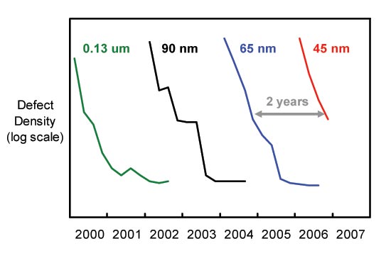
As you can see, 45nm is on a curve very similar to that of Intel's 65nm process, which means that things are on track for a smooth introduction later this year barring any unforeseen issues.
Intel attributed the rough patches in the 90nm trend to difficulty associated with building the first strained silicon transistors and using low-k interconnect dielectrics. By comparison, 65nm and 45nm appear to be much smoother sailing.
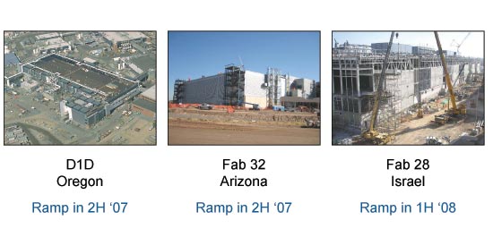
By the end of this year the first 45nm chips will be built at two 300mm Intel fabs: D1D in Oregon and Fab 32 in Arizona. Starting in the first half of 2008, Fab 28 in Israel will begin producing 45nm parts and should reach full capacity by the end of the year.
Final Words
It's very rare to get this much information out of Intel this far in advance of an actual product launch, but we're not complaining. By the middle of this year, AMD will launch its next-generation microarchitecture that will hopefully be a far better competitor to Intel's Core 2 processors. But before the year is out, Intel will respond yet again with its Penryn family of processors. We're unsure exactly what segments will be targeted first with Penryn, but by sometime in 2008 you should be able to get Penryn based notebooks, desktops and servers.
The inevitable comparison to AMD's progress on 45nm has to be made, but at this point we don't know too much. AMD revealed its 45nm SRAM test vehicle about three months after Intel did last year, with a slightly larger SRAM cell size (0.370 um^2 vs. 0.346 um^2 for Intel). The main focus for AMD at this point is the transition to 65nm; we're finally starting to see Brisbane cores available for purchase, but the highest clock speed offerings are still built on 90nm.
For Intel, we see continued strengthening and a roadmap that has a lot of promise. Penryn should be out sometime in the second half of this year, followed by a brand new architecture under the codename Nehalem. Nehalem will also be the first time we get to see an architecture change post-Core 2 under Intel's new tick-tock model of introducing new architectures every two years. It's quite possible that in the next two years Intel will have made the CPU industry far more exciting than it has been in the previous five (Core 2 launch withstanding).


59 Comments
View All Comments
quidpro - Monday, February 26, 2007 - link
What is Glaze? google is not helping.Hoser McMoose - Wednesday, January 31, 2007 - link
The calculation for the number of transistors for cache is off by a fairly significant amount in this article! The article states 288M transistors for 6MB of cache, which is FAR too low!Actual transistors for 6MB cache, if we assume ZERO redundancy is:
6MB * 1024KB/MB * 1024B/KB = 6,291,456 bytes
6,291,456 bytes * 9 bits/byte = 56,623,104 bits (remember ECC makes it 9 bits, not 8)
56,623,104 bits * 6 bits/transistor ~= 340M transistors
In reality it is actually probably more like 350 or 360M transistors required for 6MB of L2 cache since you always want a bit of redundancy. It's a bad thing if you have to throw out an entire chip due to a single bit error in your 6MB of cache!
Now, taking those numbers, if we assume that the 410M Transistor figure is accurate, the change in transistors from Conroe to Penryn is a bit different.
Conroe has 291M transistors of which at least 226M are L2 cache. That leaves only 65M assuming no redundancy, or maybe more like 50M transistors with a few redundant cache cells. According to www.sandpile.org (and I have no idea what their source is) each core of the Core 2 Duo has only 19M logic transistors. If this is accurate then it's actually HUGELY impressive, since that is WAY less then either the Pentium 4 or the Athlon64.
Murst - Monday, January 29, 2007 - link
"Intel isn't disclosing how thick the Hafnium gate dielectric layer is in its 45nm transistors, but we do know that it is thicker than the 1.2nm SiO2 gate dielectric used in previous 90nm and 65nm transistors."Why would intel make the gate larger in a shrink? Is this a typo, or is there some huge benefit to this?
IntelUser2000 - Tuesday, January 30, 2007 - link
The reason is that making the gate dielectric thinner than 1.2nm is not a good idea. 1.2nm dielectric is already equivalent to 5 atoms in thickness. Electrons can literally squeeze through the dielectric "insulator" because the dielectric is so thin. Because the material used for the dielectric layer is different from the 65nm generation, they can make the dielectric thicker without sacrificing speed characteristics. So they can increase speed AND have substantially less leakage.
Visual - Monday, January 29, 2007 - link
So, I'm a bit out of the loop lately, can anyone brief me up?Are there any new sockets, chipsets, ram changes or anything expected together with these new 45nm goodies? Or will I be fine getting a new system come Q2, and upgrading to Penryn when it's out and affordable?
ceefka - Monday, January 29, 2007 - link
I wonder if booting OXS with the new chip indicates that PC-users can soon use OSX too without having to buy a Mac. That would allow to mix and match a bit more with apps.Netopia - Sunday, January 28, 2007 - link
100 * 100 =10,000
50 * 50 = 2,500
That's a 4x improvement, not a 2x!
Joe
coldpower27 - Sunday, January 28, 2007 - link
That is not how it works...65 x 65 = 4225
45 x 45 = 2025
2025/4225 = 48% the size of the 65nm part, so close to 2x smaller.
IntelUser2000 - Sunday, January 28, 2007 - link
That's the theory. Intel's 45nm 6T SRAM size is 0.346um, and 65nm SRAM cell size is 0.57um. That's only 39% reduction(61% of the size). In addition, SRAM, which is used for cache, has the best potential for scaling. The cores will have likely worse scaling than 61%.
coldpower27 - Monday, January 29, 2007 - link
Yes, I was just presenting the mathematical example of the calculation, I wasn't going into having real world factors involved. Since in this article Anandtech simplified things with just the 2x smaller statement.