NVIDIA's nForce 420/220: It's finally here
by Anand Lal Shimpi on September 24, 2001 8:26 AM EST- Posted in
- CPUs
nForce: The Architecture
In spite of the rumors that were spread, the final nForce chipset is no different than what we reported on in our original article. The chipset is very unique because it is a clear departure from the conventional role a chipset plays in today's PC. While we won't go into too much depth here since we have covered its architecture in great detail already, it is worth noting that there are a few key points to keep in mind when looking at the nForce.
The chipset is split into two parts, as are most of today's chipsets; the Integrated Graphics Processor (IGP) and the Media & Communications Processor (MCP). With the release of the GeForce 256 "GPU", NVIDIA has been on a roll with calling everything possible a "processor" but in the case of the nForce they have very good reason to.
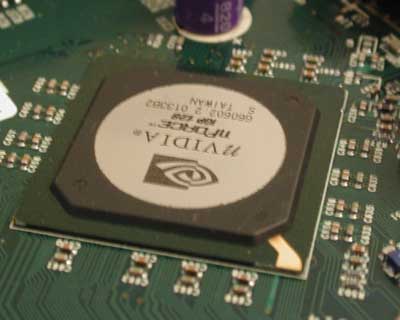
The IGP assumes the role of the conventional North Bridge or Memory Controller Hub (MCH - Intel chipsets) in a chipset. This role is generally to house an interface to the processor, AGP graphics, memory and an interface to the South Bridge or I/O Controller Hub (ICH – Intel chipsets). NVIDIA took the role of the North Bridge one step further with the IGP:
TwinBank Memory Architecture
The IGP-128 features two independent 64-bit SDR/DDR SDRAM memory controllers. In contrast, all other chipsets with DDR SDRAM support only have a single 64-bit DDR SDRAM memory controller. The benefit of having two 64-bit controllers is that you get twice as much memory bandwidth; the only constraint being that you must use two 64-bit DIMMs in order to achieve the 128-bit width which makes sense. In the case of the current nForce, the added bandwidth of going to a dual channel (via two controllers) DDR SDRAM memory bus is not really used. The reason being that the Athlon's FSB can only provide bandwidth equivalent to one 64-bit DDR266 SDRAM channel (2.1GB/s) not two (4.2GB/s). This makes the IGP-64, with only a single 64-bit SDR/DDR SDRAM controller, much more sensible for most users.
Integrated GeForce2 MX Graphics
Both versions of the IGP (IGP-128 and IGP-64) feature an integrated GeForce2 MX core running at 175MHz. This is what gives the IGP its name and it's also what makes the added bandwidth of the TwinBank Memory Architecture useful. The biggest performance constraint when dealing with integrated video solutions is memory bandwidth; there's simply not enough. Although the GeForce2 MX graphics core shares the same memory bandwidth as the rest of the system in the case of the nForce, there is enough spare memory bandwidth to offer performance very close to that of a regular GeForce2 MX. Remember that a regular GeForce2 MX has 2.7GB/s of memory bandwidth through a 128-bit SDRAM interface running at 166MHz. While the integrated GeForce2 MX on the nForce can theoretically have up to 4.2GB/s of bandwidth dedicated to itself but we all know that the CPU and peripherals will eat into that bandwidth. Realistically, at least half of that bandwidth should be available for the integrated core to use.
The amount of system memory that will be used for the GPU's frame buffer is selectable from within the BIOS. NVIDIA's reference board only allows a maximum of 32MB to be allocated at this point but even they will admit that 64MB is overkill for today's games.
The IGP also has an internal AGP bus that can be clocked at 100MHz (instead of the 66MHz clock for normal AGP buses) for transfer rates equivalent to an AGP 6X mode. While the integrated GPU will rely on the TwinBank memory controllers to provide a path to its shared frame buffer, as soon as that frame buffer is exceeded or data is requested to be transferred over the AGP bus the data will flow over this internal 100MHz AGP bus. No games today are triangle setup intensive enough to actually see a gain in performance with this 100MHz internal AGP bus, but future versions of the nForce chipset could prove the feature to be useful when more triangle data is sent between the CPU and GPU over the AGP bus.
Of course you're not constrained to use the integrated GPU and NVIDIA has included an external AGP 4X interface (operating at 66MHz) with the IGP for just this purpose. Any AGP card will work in the nForce's external AGP slot so long as it is keyed for 1.5V operation. The only recently cards not keyed for 1.5V operation are the former 3dfx Voodoo4 and Voodoo5 cards which won't physically fit in the AGP slot.
Dynamic Adaptive Speculative Pre-Processor (DASP)
Much like Intel's 845 chipset, nForce features an intelligent 8-way set associative prefetch cache in the IGP to reduce latency by looking at data access patterns and prefetching data into this cache before the CPU or GPU needs it. If the data ends up being useful, it is already cached and thus much quicker to retrieve; if it isn't useful it is just as easily discarded with no harm done.
nForce Media & Communications Processor
The power doesn't stop at the IGP; the Media & Communications Processor (MCP) of the nForce is also a very powerful part of the package. The conventional role played by the South Bridge is to provide legacy connectivity to older buses, to provide PCI, IDE and USB interfaces, and sometimes integrated Ethernet/audio controllers. The nForce MCP takes that one step further by including the most powerful integrated audio processor available to date.
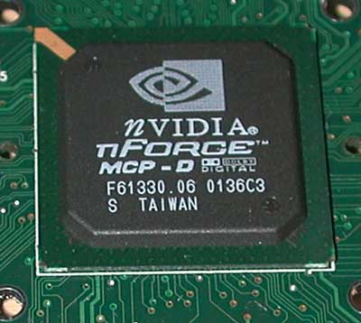
The MCP is outfitted with what NVIDIA calls their Audio Processing Unit (APU), a licensed implementation of Parthus' MediaStream DSP. In order to deal with licensing issues a separate version of the MCP named MCP-D is produced with support for real time Dolby Digital Encoding. In reality, there is no difference between the hardware of the MCP and the MCP-D it's just that in the latter case, Dolby Digital Encoding is enabled.
The MCP is connected to the IGP through the very first publicly available implementation of AMD's HyperTransport technology. For more information about the MCP, HyperTransport and the rest of the nForce architecture take a look at our nForce Preview.


1 Comments
View All Comments
Dr AB - Sunday, May 10, 2020 - link
Max Payne - Brings a lot of good memories from that era. Running it at 1024x768 at max quality and getting ~30 fps? Really impressive for a iGPU of that time.I remembr playing it on Pentium III 500 with ATI Radeon Pro AGP 2X 4MB. Performance was really terrible due to texture swapping .. even at 800x600.