Intel's Atom Architecture: The Journey Begins
by Anand Lal Shimpi on April 2, 2008 12:05 AM EST- Posted in
- CPUs
The Atom processor's architecture is not about being the fastest, but being good enough for the tasks at hand. A product like ASUS' EeePC would not have existed 5 years ago, the base level of system performance simply wasn't great enough. These days, there's still a need for faster systems but there's also room for systems that aren't pushing the envelope but are fast enough for what they need to do.
The complexity of tasks like composing emails, web browsing and viewing documents is increasing, but not at the rate that CPU performance is. The fact that our hardware is so greatly outpacing the demands of some of our software leaves room for a new class of "good enough" hardware. So far we've seen a few companies, such as ASUS, take advantage of this trend but inevitably Intel would join the race.
One of my favorite movies as a kid was Back to the Future. I loved the first two movies, and naturally as a kid into video games, cars and technology my favorite was the second movie. In Back to the Future II our hero, Marty McFly, journeys to the future to stop his future son from getting thrown in jail and ruining the family. While in the future he foolishly purchases a sports almanac and attempts to take it back in time with him. The idea being that armed with knowledge from the future, he could make better (in this case, more profitable) decisions in the past.
I'll stop the analogy there because it ends up turning out horribly for Marty, but the last sentence sums up Intel's approach with the Atom processor. Imagine if Intel could go back and remake the original Pentium processor, with everything its engineers have learned in the past 15 years and build it on a very small, very cool 45nm manufacturing process. We've spent the past two decades worrying about building the fastest microprocessors, it turns out that now we're able to build some very impressive fast enough microprocessors.
The chart below tells an important story:
| Manufacturing Process | Transistor Count | Die Size | |
| Intel Pentium (P5) | 0.80µm | 3.1M | 294 mm^2 |
| Intel Pentium Pro (P6) | 0.50µm | 5.5M* | 306 mm^2* |
| Intel Pentium 4 | 0.18µm | 42M | 217 mm^2 |
| Intel Core 2 Duo | 65nm (0.065µm) | 291M | 143 mm^2 |
| Intel Core 2 Duo (Penryn) | 45 nm | 410M | 107 mm^2 |
In 1993, it took a great deal of work for Intel to cram 3.1 million transistors onto a near 300 mm^2 die to make the original Pentium processor. These days, Intel manufacturers millions of Core 2 Duo processors each made up of 410 million transistors (over 130 times the transistor count of the original Pentium) in an area around 1/3 the size.
Intel isn't stopping with Core 2, Nehalem will offer even greater performance and push transistor counts even further. By the end of the decade we'll be looking at over a billion transistors in desktop microprocessors. What's interesting however isn't just what Intel can do to push the envelope on the high end, but rather what Intel can now do with simpler designs on the low end.
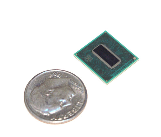
What's possible today on 45nm...
With a 294 mm^2 die size, Intel could not manufacture the original Pentium for use in low cost devices however, today things are a bit different. Intel doesn't manufacture chips on a gigantic 0.80µm process, we're at the beginnings of a transition to 45nm. If left unchanged, Intel could make the original Pentium on its latest 45nm process with a die size of less than 3 mm^2. Things get even more interesting if you consider that Intel has learned quite a bit in the past 15 years since the debut of the original Pentium. Imagine what it could do with a relatively simple x86 architecture now.


46 Comments
View All Comments
adntaylor - Tuesday, April 8, 2008 - link
On that chart with price / power, you need to be clearer...For price, you show the combined price for CPU + Chipset. For power, you say just the CPU... so 0.65W for the CPU... but you're conveniently ignoring the >2W figure for the chipset!!! This absolutely flatters Intel wherever possible.
AMD are just as misleading - they describe the Geode LX as "1W" which excludes the non-CPU core parts of the chip (which is an integrated CPU + GMCH)
Just please be honest - the figures are out there in the Intel datasheets... it takes 10 minutes to check.
Clauzii - Friday, April 4, 2008 - link
I still have a PowerVR 4MB addon card, runnung in tandem with a Rage128Pro. Quite a combination w. 15 FPS in Tombraider. Constant(!) 15FPS, that is..Amazing what they actually achieved back in 95!
Clauzii - Friday, April 4, 2008 - link
Ooops!Totally misplaced that. Sorry.
wimaxltepro - Friday, April 4, 2008 - link
The Atom represents a shift in processor architecture that is the most dramatic departure for Intel since introduction of x86 processors... the philosophy of how computing itself occurs from centralized processors to distributed processing based on an extension of the popular x86 instruction set.The Atom is not about the immediate prospects for the Atom or Nehalem products: we will likely see members of Intel's new product family be used in embedded applications in consumer products and in areas where specialized communications processors are more the rule. While not optimized for use in specific networking applications, the products capitalize on the wide range of support available in IT/Networking to develop common functions that leverage the low cost, low power/processing capability to be used as a common denominator for a wide range of applications.
Intel has been built on the 'Wintel' architecture: massively integrated chips needed to handle the massively integrated operating systems and applications of Windows (and Apple) environments. The Atom allows migration and broadening out from that architectural motif to a very highly distributed architecture. So, the increased parallelism found in the internal chip architecture is enabling of changes in external system architectures and device applications that go well beyond the typical domain of Intel.. and right into the domain of 'personal wireless broadband' and SDWN, Smart Distributed Wireless broadband Network.
The decisions about in-order vs. out of-order instruction streams, memory architecture, I/O architecture have been made in light of the broad vision for how computing, networking and, out of hand, how wireless enabled broadband networking including WiMAX will occur. This should be understood for what it represents as a shift in direction for Intel both in response to broad industry shifts and as a trend setting development.
jtleon - Friday, April 4, 2008 - link
Thanks to all the flash player ads, etc., a mobile web device will continuously avoid switching to low power states. Thus one could argue that advertising will be carbon footprint enemy of the internet's future. This is already becoming the case for desktop/laptop machines.Without such continuous (arguably wasted) consumption of CPU power, then Intel's engineered power management might have a significant impact on the value of the Atom.
Regards,
jtleon
0WaxMan0 - Friday, April 4, 2008 - link
I am definatly much impressed and enthused by intels work here, the future looks interesting esp for those of us who like low power cross compatible computing products.However I have to point out that a low power modern x86 cpu has allready been done infact 4 years ago with AMD's Geode. While technically much weaker than the Atom and with out any where near the scalability (single core design etc.) the Geode has been available in the same TDP ranges for a good long while. Take a look here http://www.amdboard.com/geode.html">http://www.amdboard.com/geode.html for some old stuff.
I do hope that the Intel name and hype makes more of an impact than AMD managed.
whycode - Thursday, April 3, 2008 - link
Does the TDP quoted include the chipset? Or is that CPU only?IntelUser2000 - Thursday, April 3, 2008 - link
Anand, the Pentium M does not feature Macro Ops Fusion. Its Core 2 Duo that started Macro Ops Fusion.Anand Lal Shimpi - Thursday, April 3, 2008 - link
You're correct, I was referencing micro-op fusion. I've made the appropriate correction :)Take care,
Anand
squito - Wednesday, April 2, 2008 - link
Am I the only one shocked to see that Poulsbo is a 130nm part...