The iPad Pro Preview: Taking Notes With iPad Pro
by Joshua Ho & Ryan Smith on November 11, 2015 7:00 AM ESTThe A9X SoC & More To Come
Finally, as everyone is undoubtedly eagerly anticipating our look at the A9X SoC inside the iPad Pro, let’s take a very quick look at what we know about the SoC so far. There’s a bit of a limit to what we can do blindly via just software, but I’m hoping that the eventual A9X die shots will confirm some of our suspicions on A9X’s configuration.
| Apple SoC Comparison | ||||||
| A9X | A9 | A8X | A6X | |||
| CPU | 2x Twister | 2x Twister | 3x Typhoon | 2x Swift | ||
| CPU Clockspeed | 2.26GHz | 1.85GHz | 1.5GHz | 1.3GHz | ||
| GPU | PVR 10 cluster Series7? | PVR GT7600 | Apple/PVR GXA6850 | PVR SGX554 MP4 | ||
| RAM | 4GB LPDDR4 | 2GB LPDDR4 | 2GB LPDDR3 | 1GB LPDDR2 | ||
| Memory Bus Width | 128-bit | 64-bit | 128-bit | 128-bit | ||
| Memory Bandwidth | 51.2GB/sec | 25.6GB/sec | 25.6GB/sec | 17.1GB/sec | ||
| L2 Cache | 3MB | 3MB | 2MB | 1MB | ||
| Manufacturing Process | Unknown (TSMC 16nm or Samsung 14nm) |
TSMC 16nm & Samsung 14nm |
TSMC 20nm | Samsung 32nm | ||
First and foremost, the most unexpected news here is that unlike A8X, A9X is not packing a triple-core CPU. Instead A9X drops back down to just a pair of Twister CPU cores. The twist here is that relative to A8X and A9, Apple has cranked up their CPU clockspeeds. Way, way up. Whereas the iPad Air 2 (A8X) shipped at 1.5GHz and the iPhone 6s (A9) at 1.85GHz, the A9X sees Apple push their clockspeed to 2.26GHz. Not counting the architectural changes, this is 22% higher clocked than the A9 and 51% higher than the A8X.
The fact that Apple dropped back down to 2 CPU cores is unexpected given that we don’t expect Apple to ever go backwards in such a fashion, and while we’ll never know the official reason for everything Apple does, in retrospect I’m starting to think that A8X was an anomaly and Apple didn’t really want a tri-core CPU in the first place. A8X came at a time where Apple was bound by TSMC’s 20nm process and couldn’t drive up their clockspeeds without vastly increasing power consumption, so a third core was a far more power effective option.
By comparison, with the FinFET process Apple is using here – and given the lower volume of A9X I don’t have reason to believe it’s dual-sourced, so it’s either TSMC or Samsung – Apple has been free to increase their clockspeeds substantially. At the same time these FinFET processes are still new and yields won’t be great, so there is a strong incentive to keep die sizes down to keep yields up, and adding a third core would only make that harder. If I had to guess, Apple only wanted two cores to begin with – this makes it easier for developers knowing that they only have two cores to work with – and that it’s A8X that is the anomaly.
Otherwise a highly clocked CPU is far more in-line with Apple’s design philosophy as it means that A9X is capable of amazing single-threaded performance – and keep in mind that we’re talking ARM Cortex-A57-like clockspeeds for a CPU that gets much more work done per cycle – so what we see here makes a lot of sense. Plus with iPad Pro in particular Apple has more battery capacity to sustain the power draw of a higher clocked SoC, and more surface area to dissipate that heat, so the usual concerns about power and cooling aren’t quite as pressing. I do wonder if this will impact multitasking performance much, but given what Twister is capable of, I’m not nearly ready to write off a dual-core Twister implementation clocked this high.
Moving on, as is customary for the X-series SoCs from Apple, A9X features what I believe to be a wider 128-bit LPDDR4 memory bus. The memory bandwidth numbers clearly point to a wider bus, and Apple needs the bandwidth to feed a more powerful GPU.
| Geekbench 3 Memory Bandwidth Comparison (1 thread) | ||||||
| Stream Copy | Stream Scale | Stream Add | Stream Triad | |||
| Apple A9X 2.26GHz | 20.8 GB/s | 15.0 GB/s | 15.3 GB/s | 15.1 GB/s | ||
| Apple A8X 1.5GHz | 14.2 GB/s | 7.44 GB/s | 7.54 GB/s | 7.49 GB/s | ||
| A9X Advantage | 46.4% | 101% | 103% | 102% | ||
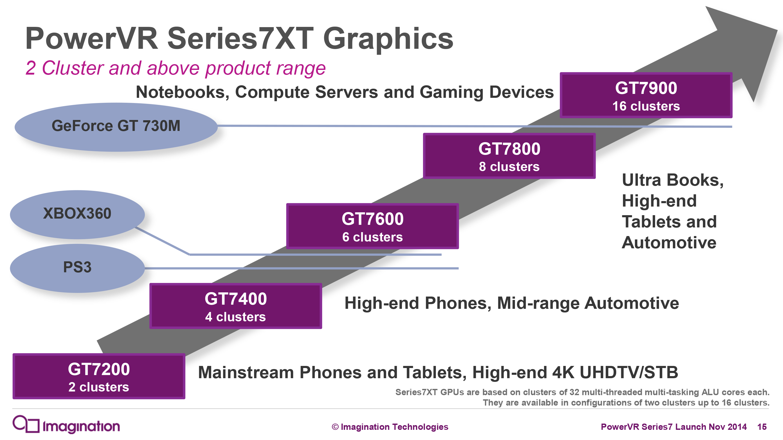
Which brings us to the last bit of our preview, the GPU. Apple went with a 6 cluster PowerVR Series7 design on A9, and for A9X they have gone with a larger design. Without a die photo it’s basically impossible to determine how many clusters are in use since clockspeed plays such an important role. What we do know is that GPU performance relative to A9 has pretty much doubled, which once again is right in-line with Apple’s usual design goals.
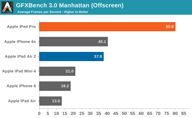
Given what Apple has done with clockspeed on Twister, for the moment I am staking my bet on it being a 10 cluster design with a higher GPU clockspeed than A9 giving us the rest of the performance boost. To be clear here this could also be a 12 cluster design at a similar clockspeed or even an 8 cluster design clocked far higher – we’ll need die shots to confirm – but given all of the options it’s a 10 cluster design that is the best balance between die size and clockspeed, and it would also be the biggest curveball Apple could throw. It should also be noted that PowerVR Series7 certainly supports such a configuration since it’s scalable from 2 to 16 clusters, although in Imagination’s official product catalog they don’t have a name for such a configuration. So for the moment I’m simply calling it a 10 cluster Series7.
Anyhow, we’ll be back later with a full review of the iPad Pro, including the pros and cons of Apple’s first large-format, productivity-oriented tablet, and a full breakdown of the A9X SoC. So until then stay tuned.


199 Comments
View All Comments
Aenean144 - Wednesday, November 11, 2015 - link
A few months ago, the criticism against ARM was that it had native AES instructions and that's why it is competitive to Intel x86. Now that people actually looked at the GB subscores and see that lo and behold, Intel has awesome AES scores relative to ARM, the criticism has moved on to SHA subscores.Give it a break. There's like 13 integer sub-benches. Removing one won't change the scores much. Plus, it's a tautological criticism: this CPU won't be that fast if remove the things that it is good at from the benchmarks. Next thing you're going to tell me is that ARM is cheating by have large caches?
That big cache criticism has been making the rounds too.
xthetenth - Wednesday, November 11, 2015 - link
That sort of thing is the downside of the lack of multiplatform benchmarks. It makes it really tricky to determine which things are quirks of the benchmark and which are really indicative of greater trends in performance.Aenean144 - Wednesday, November 11, 2015 - link
That's no such thing as a blackbox benchmark, where you run it and show the results. You won't find "good" multi-platform benchmarks unless it tests simpler things, like graphics ops. Testing of the applications you most use is always the best benchmark because compilers have such a big effect, but that apparently takes too much work and time.The big issue with mobile and handset testing is the vast mass of tech media that review products have zero understating of the benchmarks they use, have no desire to learn what they mean, and thusly lead them to say stupid shit because all they want to do is the simple blackbox comparison of device A has a better score than device B, therefore better.
I've basically stopped reading reviews as 99% of them have no value.
Morawka - Tuesday, November 17, 2015 - link
Prime Numbers and Memory Bandwidth should be all we need to see how good a CPU/SOC isbeginner99 - Thursday, November 12, 2015 - link
Somewhat true and we aa HW enthusiasts want to compare the hardware regardless of real-world usage. However for a consumer stuff like Geekbench is irrelevant. In a mobile I buy the whole platform and hence I compare an Samsung Phone with Samsung SOC and Android to an IPhone with an Apple SOC and iOS.Hypothetically: If the Apple SOC is faster but say sucks in browser benchmarks because Safari (or iOS) sucks, too bad. I don't care that the apple SOC is theoretically much faster. I buy the platform that as a whole is faster.
id4andrei - Wednesday, November 11, 2015 - link
Linus Torvalds would like a word with you."Geekbench is SH*T.
It actually seems to have gotten worse with version 3, which you should be aware of. On ARM64, that SHA1 performance is hardware-assisted. I don't know if SHA2 is too, but Aarch64 does apparently do SHA256 in the crypto unit, so it might be fully or partially so.
And on both ARM and x86, the AES numbers are similarly just about the crypto unit.
So basically a quarter to a third of the "integer" workloads are just utter BS. They are not comparable across architectures due to the crypto units, and even within one architecture the numbers just don't mean much of anything.
And quite frankly, it's not even just the crypto ones. Looking at the other GB3 "benchmarks", they are mainly small kernels: not really much different from dhrystone. I suspect most of them have a code footprint that basically fits in a L1I cache.
Linus"
tipoo - Wednesday, November 11, 2015 - link
Linus's statement confused me, for surely he must know Geekbench uses a geometric mean, so singular high scores don't skew the overall score much.id4andrei - Wednesday, November 11, 2015 - link
I see it as an indication that the test is too simple(workload/data sets etc.) to be meaningful in the sense that it's the definitive bench that decided which ISA is faster/better. That's before getting into score calculation.Linpack is another crossplatform bench that favors x86 more. Why aren't we using that?
Dmcq - Thursday, November 12, 2015 - link
A four times advantage in one test will give a 4^(1/13) = 11% advantage in the integer test and about 4% overall so it isn't inconsequential. At least it isn't quite as bad as the difference libquantum makes in SPECint2006 where a compiler noticing the trick to optimize it can easily make the overall result a third higher.Aenean144 - Wednesday, November 11, 2015 - link
Yes, Linus calls a lot of things shit, most of the time for dramatic effect.He will admit that Apple's ARM architecture is competitive.