The Intel Skylake Mobile and Desktop Launch, with Architecture Analysis
by Ian Cutress on September 1, 2015 11:05 PM ESTIf you read our review of the Skylake-K processors, you will note that in terms of clock-for-clock performance, Skylake was not as big of a jump as people were perhaps expecting, affording an average of 5.7% over Haswell and 2.7% over Broadwell. For an architecture change, users (us included) have come to expect a 5-10% generation on generation increase at the same frequency. So by getting these results, we started to point some fingers and questions at Intel regarding the architecture due to the fact that in a change from previous launches this information was to be provided post-launch. That time was IDF, and while Intel did get somewhat technical, there are still some questions hanging in the air. In the meantime, this is what we learned. For this page, we’re focusing purely on performance, with power considerations a few pages further on.
Do More On The Fly
There are many different metrics and underlying on-paper ways to increase performance. Being able to process commands and data in fewer cycles, or by handling/processing more data at once, are two very important ones. Intel tries to tackle both within the out-of-order architecture.

Instruction level parallelism is one of the holy grails in processor design – if you are able to separate a set of code into X instructions and process all X at once (due to a lack of dependencies), then the problem is cracked. The downside is that a lot of code and as a result, a lot of instructions, rely on other instructions and data. The best bit about an out-of-order architecture is that when many different branches of code and instructions are in flight at once, they can be grouped up in the scheduler and a level of instruction parallelism can be achieved.
So first up is the OoO window, increasing 16.7% over Haswell. This allows the micro-ops (Intel’s version of deconstructing the instructions) to fill the queue and be arranged such that more parallelism can take place. This also takes advantage of in-flight loads and stores such that data can be available by the time the micro-op gets to the front of that queue. The idea is that heavy workloads that are interchangeable but require data access stalls can take advantage and hide the latency associated with those stalls, as well as allowing certain operations to be fused in order to reduce the workload.
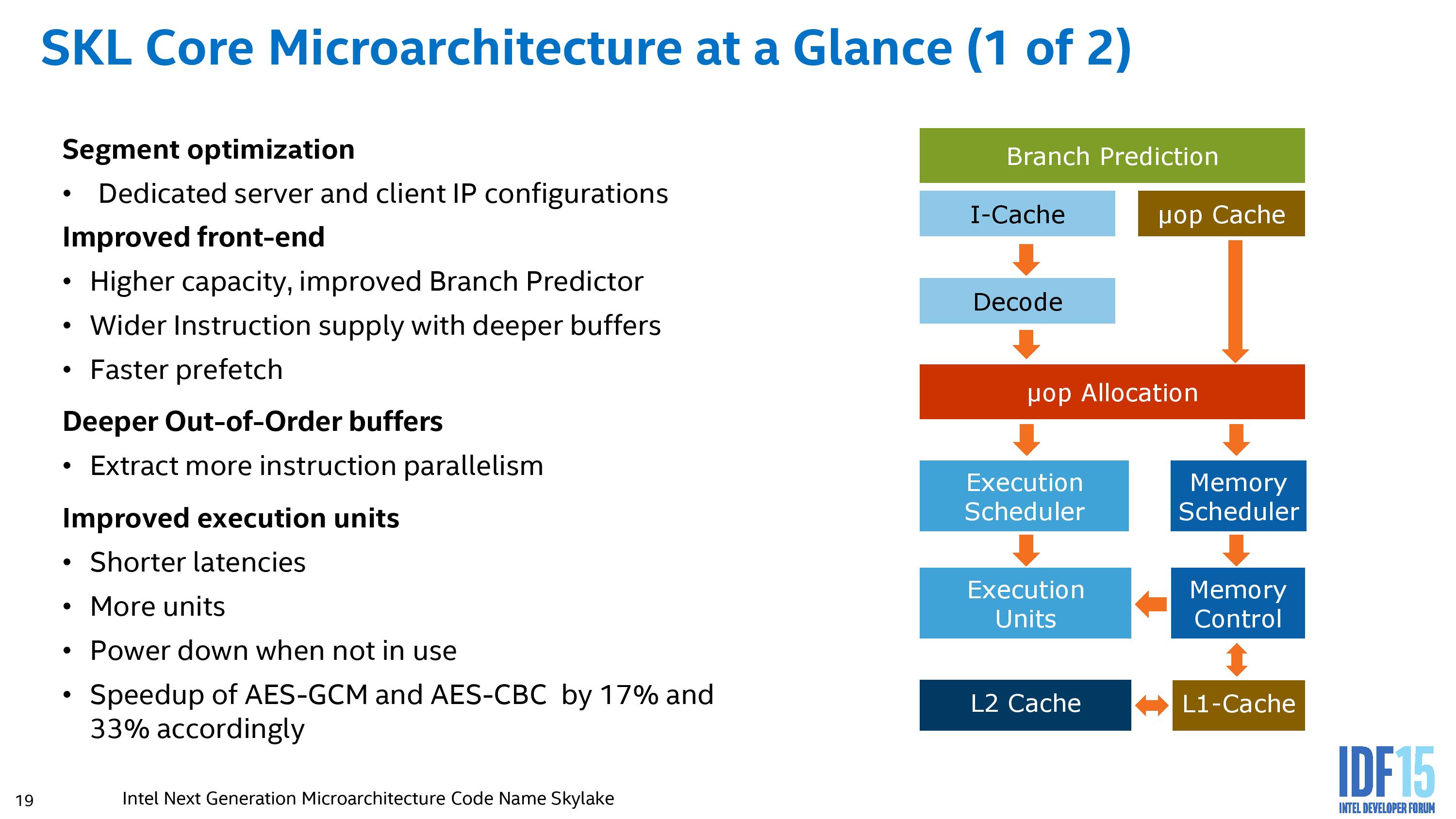
With the micro-ops, Intel has upgraded the front end of the IA core to allow a dispatch of six micro-ops at once, up from four on Haswell. This allows the queue to be quicker, but also the dispatch of micro-ops from the queue to the execution units has increased to six also. Note that the execution units are limited by the number of INT/FP/Load/Store available, so it is the job of the queue to reorder the micro-ops to take advantage of this, as well as manage the memory accesses.
The front-end (uOp allocation and up) is designed to take advantage of better branch prediction and faster prefetch, as well as the increased in-flight buffers as mentioned above. Branch prediction is also another element to increasing processor performance here – in some circumstances the CPU will speculate as to the instruction required and then dump the result it doesn’t need. Too much speculation wastes power, but not enough will result in increased processing time and latency. So the branch predictor acts as a secret sauce for a lot of core design, but we are told that Skylake improves this.
On the front end, there are some small adjustments in the execution units with regards latency – the divider is improved, which is normally a difficult set of commands to optimize and calculated via an improved radix. Typically when writing scientific calculation code for example, it is often suggested to minimize divisions where possible. On the other side of the coin, the FMUL (floating point multiply) has increased in latency over Broadwell, and returned to the same as Haswell. We are told that this is due to design decisions that allows for better performance when it comes to creating enterprise silicon, which is an interesting explanation in itself. The execution units also have a greater degree of granularity in their power modes, allowing those not active to save power.
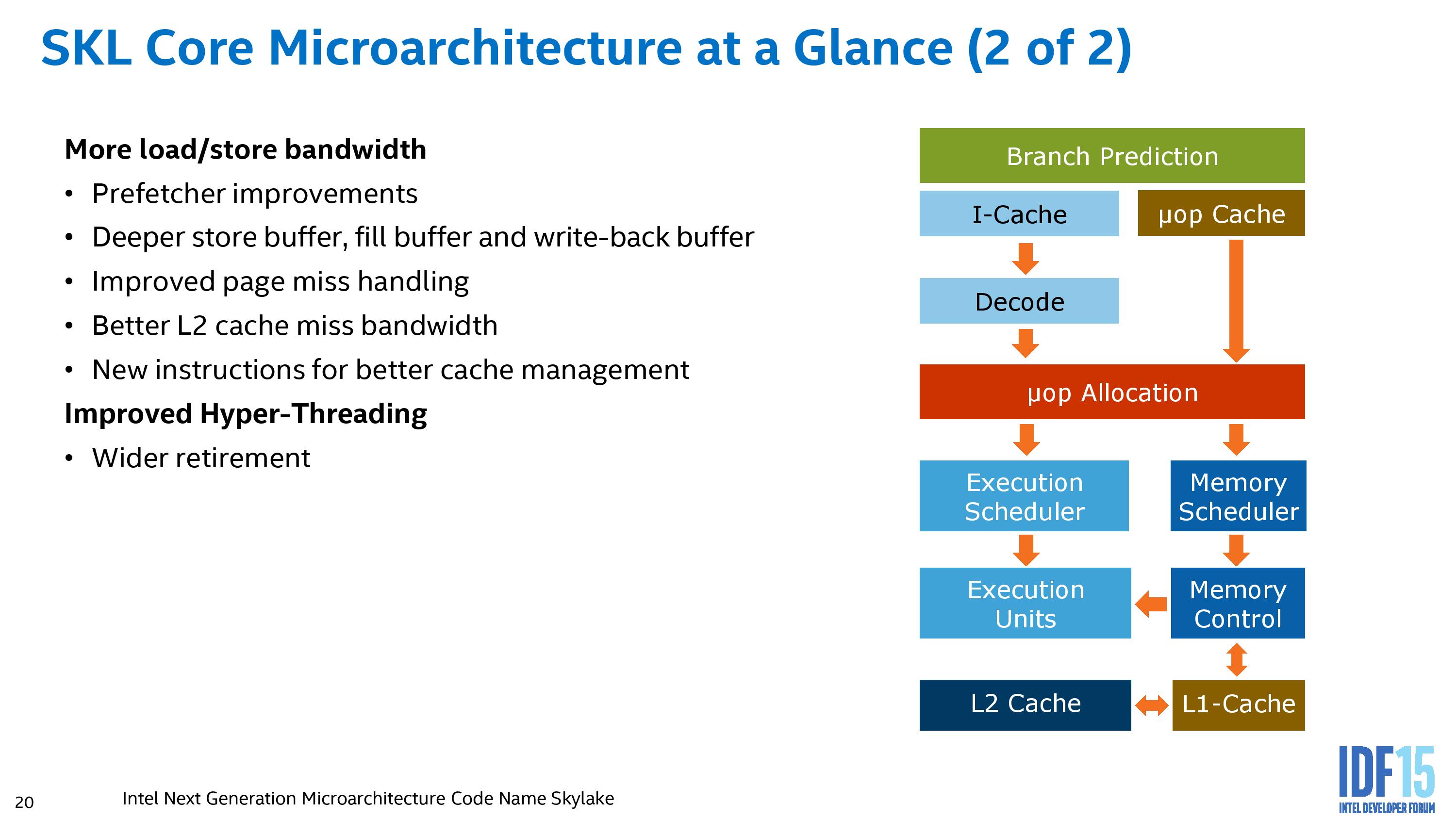
One element we did not mention in our original Skylake review (because we didn’t notice, I’ll be honest), is that the L2 cache on Skylake is reduced from an 8-way associative cache to a 4-way model. This is odd for Intel, given that as far back as Sandy Bridge, they have always worked with an 8-way L2. In real world terms, this relates to how the L2 data is stored and accessed, where a doubling in the associativity often reduces the miss rate depending on the algorithm. However, reducing the associativity saves power on data accesses that are successful and in some circumstances can also save area on the silicon die. So by moving from 8-way to 4-way, Intel saves some power with Skylake but loses some performance if you compare two identical silicon models. Intel counters this move by saying that the bandwidth to the L2 cache misses is doubled, as well as improving how cache and page misses are handled providing a lower latency for that data. The end result should be performance similar to that in Haswell, but at a lower power. We were also told that this has benefits when designing the server processor line, although we will have to wait and see exactly why.
Another element to the back-end results in improved HyperThreading performance. In our benchmark data we have seen this, where for example the ratio of Cinebench single threaded performance to multi-threaded performance was better than previous generations. Part of the HT improvements relate to micro-op retirement – basically being able to abandon used operations and free up the execution queue. When I heard this, my first question was if instruction retirement was ever a bottleneck – would you ever be in a position where you have all the data you need to process an instruction but because the older instruction is not cleared, the new instruction cannot be processed? Apparently the answer is yes, and the new design allows each thread in a core to retire four micro-ops in one cycle. This should mean that HyperThreading yields some tangible benefits when it comes to intensive workloads (again, another nod to the enterprise performance crowd).
Ultimately, from a pure core design point of view, Skylake looks a lot like Haswell with minor tweaks that are not instantaneously obvious. It can be hard to feel how ‘a deeper buffer’ can increase performance when the software being used barely filled the buffer in the first place. A lot of these improvements are aimed directly at the pure-performance perspective (except L2 and FMUL to an extent), so you really have to be gunning it or have a specific workload to take advantage.
It is at this point I should mention that Intel's policy of disclosing new architecture details seems to hold back more and more details each generation, such as pipeline length, branch misprediction penalties and exact adjustments to instruction throughput. For example, the FMUL adjustment in latency was only found when we asked about it based on a rumor we had heard. It seems that Intel might be willing to give the information if specific questions are asked, although other information needs to be investigated.
A side note on the enterprise based comments. In the first slide of the core front/back end, it states ‘dedicated server and client IP configurations’. As far as we can tell, this is a drive to make Intel’s processor/core designs more modular in nature such that being able to produce a custom processor for a certain enterprise market is easier to do. That being said, designing a core and working within design constraints can be a pain (you want registers and caches to be close to the queues to be close to the execution units and so on), so some optimization in a modular system still has to be made. It also makes us wonder to what level the modularity can take, and if some of the more esoteric designs might help Intel develop custom SoCs similar to AMD. It’s a thought.
Security Technologies
Along with the core upgrades, Intel is introducing both SGX (Security Guard Extensions) and MPX (Memory Protection Extensions) to Skylake.
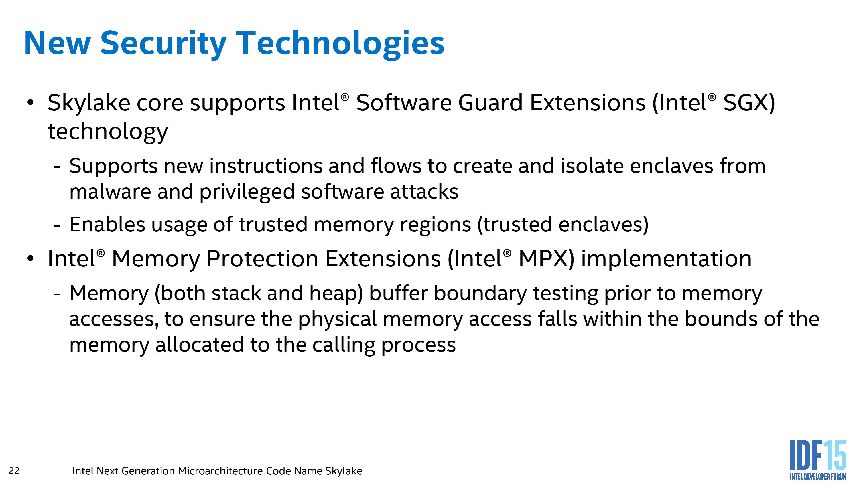
This is in part similar to ARM’s TrustZone, or sandbox modes, whereby a program can be run in its own environment (or enclave is what Intel calls it) where it cannot interact outside the enclave and any attempt by other programs to access the memory in which it resides fails.

The MPX implementation is to aid buffer overflow errors that are a common source of security breaches.


eDRAM Changes
Until testing Broadwell-H and meeting up with certain individuals at IDF, the principle of the eDRAM Intel had been using was a little ill-defined. Sure we tested it when it launched, as well as the Broadwell processors, and commented that the obvious tasks to be improved came down to gaming on integrated graphics or very specific workloads. For Skylake, eDRAM enabled processors will be configured differently to previous versions in order to make the effect of the eDRAM more seamless for software.
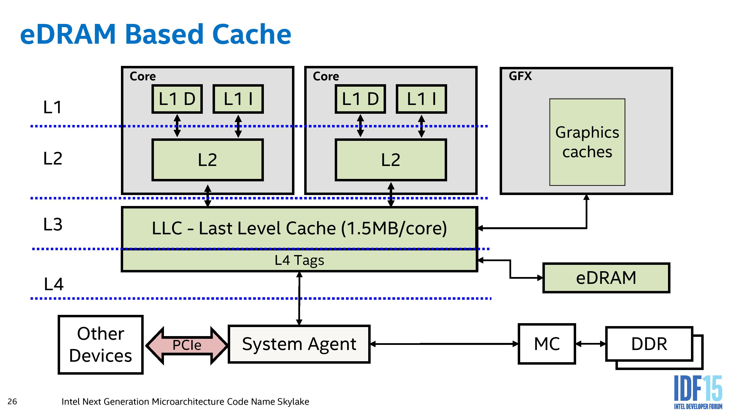
This is the current eDRAM representation for Haswell and Broadwell processors. Here we see that the eDRAM is accessed by a store of L4 tags contained within the LLC of each core, and as a result acts more as a victim cache to the L3 rather than as a dynamic random access memory implementation. Any instructions or hardware that requires data from the eDRAM has to go through the LLC and do the L4 tag conversion, limiting its potential (although speeding up certain specific workloads by virtue of a 50 GB/s per-link bi-directional interface.
In Skylake, the eDRAM arrangement changes:
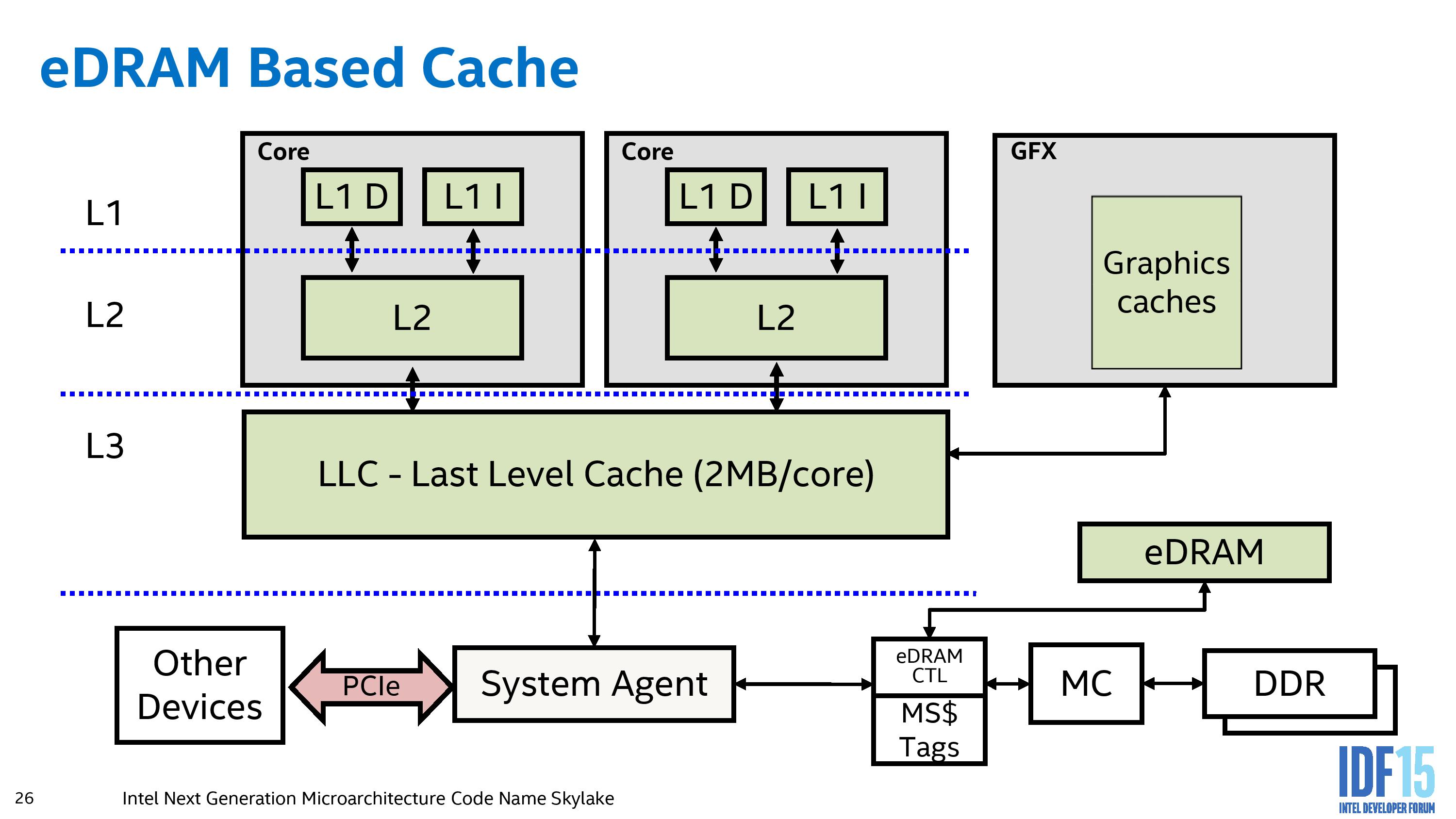
Rather than acting as a pseudo-L4 cache, the eDRAM becomes a DRAM buffer and automatically transparent to any software (CPU or IGP) that requires DRAM access. As a result, other hardware that communicates through the system agent (such as PCIe devices or data from the chipset) and requires information in DRAM does not need to navigate through the L3 cache on the processor. Technically graphics workloads still need to circle around the system agent, perhaps drawing a little more power, but GPU drivers need not worry about the size of the eDRAM when it becomes buffer-esque and is accessed before the memory controller is adjusted into a higher power read request. The underlying message is that the eDRAM is now observed by all DRAM accesses, allowing it to be fully coherent and no need for it to be flushed to maintain that coherence. Also, for display engine tasks, it can bypass the L3 when required in a standard DRAM access scenario. While the purpose of the eDRAM is to be as seamless as possible, Intel is allowing some level on control at the driver level allowing textures larger than the L3 to reside only in eDRAM in order to prevent overwriting the data contained in the L3 and having to recache it for other workloads.
As noted in the previous pages, the eDRAM from Intel will come in two flavors – 64 MB and 128 MB, which is different to the 128 MB only policy for Haswell and Broadwell. Back when Intel was discussing eDRAM before this, it was noted that Intel considered 32 MB ‘enough’, but doubled it and doubled it again just to make sure the system truly saw some benefit. It seems that for some circumstances (or some price points for that matter) 64 MB is felt as a better fit in that regard, given that Intel believes that its initial design had plenty of headroom. As far as we can tell, eDRAM will be available in 64MB for GT3e and 128MB for GT4e configurations (48 EUs and 72 EUs respectively), although we might see some variation as time goes on. We have confirmed with Intel that the 64 MB implementation is a half-silicon implementation (rather than a disabled full-silicon), but the bandwidth to the system agent is the same in both circumstances.
A number of media have already been requesting an announcement regarding a discrete processor with an eDRAM implementation, similar to Broadwell. I even enjoyed conversations at IDF where it was suggested that Intel could produce an i7 at 4.0 GHz with 128MB eDRAM, either with or without overclocking, and charge a nice $30-$50 premium for it. However, we were told that a quad core desktop part with eDRAM (either 4+2e or 4+4e) is currently not POR, which means ‘plan of record’. To avoid confusion, because technically a 3+2 is not on their ‘plan of record), having been mentioned as not POR means means that Intel has looked at it as an option but at this time has not decided to release it at this time - if they ever will is another question to ask Intel. For users who actively want an LGA1151 4+4e configuration, make sure your Intel representative knows it, because customer requests travel up the chain.


173 Comments
View All Comments
JKflipflop98 - Sunday, September 6, 2015 - link
Dude, if you're still running Arrandale, just about anything you buy at this point is going to be a *MAJOR* upgrade across the board.tipoo - Tuesday, September 1, 2015 - link
"Intel’s graphics topology consists of an ‘unslice’ (or slice common) that deals solely with command streaming, vertex fetching, tessellation, domain shading, geometry shaders, and a thread dispatcher. "This part of their architecture seemed like the weak spot which led to little scaling between 1/2/3 slices going from DX11 to DX12. So will that remain the same with Skylake, or are there other differences that will allow better scaling with DX12?
extide - Wednesday, September 2, 2015 - link
That sentence is actually incorrect (the quote).The unslice is not the same as slice common.
The Unslice is whats not in the slices, obviously, but the 'Slice Common' is what IS in the slice, but which ISNT the EU's themselves..
extide - Wednesday, September 2, 2015 - link
So, for example, GT2 has 1 Unslice, 3 Slice Commons (1/slice) and 24 EU's (8/slice).extide - Wednesday, September 2, 2015 - link
Actually it's GT2 has 1 Unslice, 1 Slice, 3 sub slices, 3 Slice Commons (1/subslice) and 24 EU's (8/subslice).ltcommanderdata - Tuesday, September 1, 2015 - link
Apple appears to take the Core M and use it in a 7 W cTDP up configuration in the Retina MacBook. I wonder if the increase in performance would be worth the increased heat and power consumption to use U-class processors in a 7.5 W cTDP down configuration instead? Or even try to accommodate 9.5 W cTDP down U-class processors to take advantage of the GT3e to better drive the retina display?Kutark - Tuesday, September 1, 2015 - link
I feel like i should know this already, but what are they referring to with the whole 4+2, 2+2 etc etc?Kutark - Tuesday, September 1, 2015 - link
Nm, i think i figured it out. 4core + GT2, or 2core +gt2, etc etcHideOut - Wednesday, September 2, 2015 - link
Yep, nailed it. (the +2/3/4 is GT2/3/4)Braincruser - Wednesday, September 2, 2015 - link
first number is CPU cores/modules, second part is gpu modules.