Samsung Announces 14nm FinFET for Exynos 7
by Joshua Ho on February 16, 2015 4:04 AM EST- Posted in
- Smartphones
- Mobile
- Tablets
- SoCs
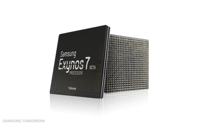
While we've known about the existence of the Exynos 7420 for a while now, we didn't really know what to expect until recently. Today, it seems that Samsung is ready to start disclosing at least a few details about an upcoming Exynos 7 SoC, which is likely to be the Exynos 7420.
At a high level Exynos 7 will have four Cortex A57s clocked at 2.1 GHz, in addition to four Cortex A53s along with an LPDDR4-capable memory interface. According to Samsung Tomorrow, we can expect a 20% increase to device performance, which is likely a reference to clock speed, and 35% lower power consumption. In addition, there is a reference to a 30% productivity gain, which is likely to be referencing performance per watt. Samsung claims that these figures come from a comparison to their 20nm HKMG process, which we've examined before with the Exynos 5433 in the Note 4 Exynos review.
Although there is no direct statement of which version of 14nm is used for this upcoming Exynos 7 Octa, judging by how this is the first 14nm IC to come from Samsung it's likely that this SoC will use 14LPE, which focuses on reducing leakage and power consumption rather than switching speed.
Source: Samsung Tomorrow


111 Comments
View All Comments
witeken - Monday, February 16, 2015 - link
Let's forget that Intel has been shipping *hundreds* of millions of FinFETs since early 2012, which puts Samsung 3 years behind Intel.The only company who you can buy FinFETs from, is still Intel. Take a moment to realize this; Intel is now in its 2nd gen FinFET, while other companies have yet to ship their first generation! TSMC will only start HVM in H2 of this year.
And let's also not forget that this node shouldn't have been called 14nm in the first place by Samsung, since it uses the same 20nm feature sizes. The accurate name would be 20+FF. But marketing didn't do that because then it would seem to people that Intel will be 2 nodes ahead when it launches 10nm next year (which will indeed be the case, but now people won't know because of the FUD marketing is spreading).
toyotabedzrock - Monday, February 16, 2015 - link
Third generation, remember they had to improve things after the first 22nm parts, over clocking was improved after. And they seem set to release skylake on time or ahead of time.Would be great if anand could do an article on mpx and what it will do in skylake.
Guest8 - Monday, February 16, 2015 - link
Yeah the faux 14/16 nm parts are really 20nm with FinFETS. So the Intel lead is very much real and still intact.patrickjp93 - Tuesday, February 17, 2015 - link
Um, no. Samsungs "14nm FF" process is actually 20nm in disguise. The only company at 14nm is Intel, and it's by a huge lead. https://www.semiwiki.com/forum/content/3884-who-wi...Samsung's process at 14nm FF is 33% larger than Intel's. Sorry but Intel's > 1 year lead will remain until TSMC's 16nm FF+, and then Intel drops to true 10nm.
psychobriggsy - Monday, February 16, 2015 - link
Certainly Intel doesn't have the 2 to 3 year lead it used to have.And as this SoC will be produced in the millions (tens of millions even) - and I'm sure Apple are bringing up the A9 on the same process too (tens of millions), the yield on the process at the sizes of these mobile SoCs (100mm^2 - 150mm^2) must be good.
And 14nm yield is one of the rumoured issues of Intel's 14nm, putting it's mass release back by a year, and having the initial products be small die low-wattage parts.
However the actual real world density of the processes is still to be compared - I believe that Samsung's 14nm process uses a 20nm BEOL for a start. Things like SRAM cell size, logic transistors per mm^2, and so on.
toyotabedzrock - Monday, February 16, 2015 - link
It was a 3 month delay and it has been fixed.Guest8 - Monday, February 16, 2015 - link
More likely the yields are terrible. It's my belief that's the reason for the tech sharing with GloFo. Crappy yields but we need millions so we will just run more wafers. I will bet money there is a clause in that deal that allows Sammie to buy the output at cost if needed from GloFo in exchange for the 14nm tech to be shared. Not a bad deal for both since GloFo was in third place.TheJian - Tuesday, February 17, 2015 - link
Yields are fixed and good, that is why Apple, Qcom AND Nvidia all are going there Q2 according to many sources (samsung claims Q2 mass products from all these). In that order supposedly too, so NV stuff last, but all should make it into xmas products as it only takes 4.5-6mo to put something out with google being the best so far AFAIK at 4.5mo for nexus 7. I would be pretty happy with a 14nm shield device with maxwell and denver both with boosted clocks (which NV confirmed is on future chips - for anyone thinking Denver is gone). They explained they are on a TICK/TOCK like Intel now so went with off the shelf for time to market on X1 (and it was aimed at cars, where off the shelf IP means nothing power wise, huge car batteries).GF will benefit the most from TSMC screwup though, if sammy can't do enough for all. There deal goes both ways however. Whoever gets something fixed, the other gets it ASAP. So if Finfet+ or whatever they call it has great yields at GF, samsung gets it immediately too. I doubt there is a AT COST clause. It's a combined effort for the good of both to catch Intel (with IBM doing the groundwork first, then the two take it from there).
Guest8 - Tuesday, February 17, 2015 - link
And you know these yield numbers how? That is one of the most guarded secrets in the industry. It took me weeks to get a snippet of info on how low TSM 20nm was yielding. Yields are not fixed. They are running a ton of wafers. Only time will tell who's right by seeing much product ends up being out there. Thus far Apple A8 is the only TSM 20 nm product out there on the shelves.frenchy_2001 - Tuesday, February 17, 2015 - link
You are mixing up his answer. He talked about Samsung's yields. TSMC is having problems with their 20nm (hence why Apple pretty much has the only mass produced chip from TSMC at that size). Samsung seems to have the volume and now switched to "14nm".There is no "at cost" clause in the co-development from IBM/GloFo and Samsung. It is just *SO* expansive to keep developing foundry processes that most companies cannot do it alone. Companies owning fabs has been a shrinking list for years, even IBM got out recently. It costs BILLIONS to develop a new shrunk process and BILLIONS more to tool a fab line. This is why we can count companies fabbing at 20nm and lower on the fingers of ONE hand (Intel, TSMC, GloFo, Samsung).