GeForce GTX 970: Correcting The Specs & Exploring Memory Allocation
by Ryan Smith on January 26, 2015 1:00 PM EST
Over the weekend we reported on a statement released by NVIDIA regarding recent concern over unusual VRAM allocation and VRAM bandwidth performance from the GeForce GTX 970. In brief, various GTX 970 owners had observed that the GTX 970 was prone to topping out its reported VRAM allocation at 3.5GB rather than 4GB, and that meanwhile the GTX 980 was reaching 4GB allocated in similar circumstances. All of this was at odds with what we thought we knew about the cards and the underlying GM204 GPU, as the two cards were believed to have identical memory subsystems.
In their statement, NVIDIA confirmed that this unusual behavior existed, and that it was due to the GTX 970 possessing “fewer crossbar resources to the memory system” than the GTX 980. Furthermore due to this, the VRAM on the GTX 970 was segmented in a way it’s not on the GTX 980, with 3.5GB of the 4GB serving as one high priority segment, and the final 512MB serving as a low priority segment. The rest of NVIDIA’s statement then focused on performance, and why they believed this design would not have a significant performance impact versus a GTX 980-style non-segmented memory structure.
However because NVIDIA’s statement was intentionally high-level – it was meant to be accessible to the wider press and their readers, and not just the technical press such as ourselves – this meant that the statement offered few technical details on what was going on under the hood, which makes it difficult for us to validate NVIDIA’s claims and on a more human level we’re always dissatisfied with half of an answer.
As a result we’ve been digging into this issue over the weekend, working to collect the final pieces of the puzzle. To that end NVIDIA reached out to us Sunday evening to fully explain the issue at a level of detail necessary for our level of depth, making available to us a “triage team” of sorts of technical marketing, product management, and engineering/architectural personnel to answer questions and to better explain the issue. While there’s still some benchmarking left to do on our end – we’ve only had a relatively brief Sunday evening to work with NVIDIA’s full explanation – at this point we feel like we have a solid grasp of what’s going on with the GTX 970, how its memory segmenting and allocation work, and how it can impact performance.
Now make no mistake, NVIDIA right now is in full damage control mode due to the negative press this issue has garnered and the pain that’s going to follow. When NVIDIA is getting Senior VPs like Jonah Alben on the phone with us on a weekend night to talk architecture and answer questions, this isn’t normal operating procedure for the company. But at the same time it’s a positive sign for how serious NVIDIA is taking our concerns, and meanwhile an NVIDIA under pressure is an NVIDIA that is more likely to answer our deepest technical questions, giving us more insight than ever before into GM204.
GeForce GTX 970: Correcting the Specifications
To kick things off, we need to start at the very beginning and talk about the specifications of the GTX 970 itself. Everything that follows is derived from how the chip is configured, so we cannot go any farther until we understand the true configuration of the GTX 970.
| NVIDIA GPU Specification Comparison | |||||
| GTX 980 | GTX 970 (Original) | GTX 970 (Corrected) | |||
| CUDA Cores | 2048 | 1664 | 1664 | ||
| Texture Units | 128 | 104 | 104 | ||
| ROPs | 64 | 64 | 56 | ||
| Core Clock | 1126MHz | 1050MHz | 1050MHz | ||
| Boost Clock | 1216MHz | 1178MHz | 1178MHz | ||
| Memory Clock | 7GHz GDDR5 | 7GHz GDDR5 | 7GHz GDDR5 | ||
| Memory Bus Width | 256-bit | 256-bit | 256-bit | ||
| VRAM | 4GB | 4GB | 4GB | ||
| L2 Cache | 2MB | 2MB | 1.75MB | ||
| FP64 | 1/32 FP32 | 1/32 FP32 | 1/32 FP32 | ||
| TDP | 165W | 145W | 145W | ||
| GPU | GM204 | GM204 | GM204 | ||
| Transistor Count | 5.2B | 5.2B | 5.2B | ||
| Manufacturing Process | TSMC 28nm | TSMC 28nm | TSMC 28nm | ||
| Launch Date | 09/18/14 | 09/18/14 | 09/18/14 | ||
| Launch Price | $549 | $329 | $329 | ||
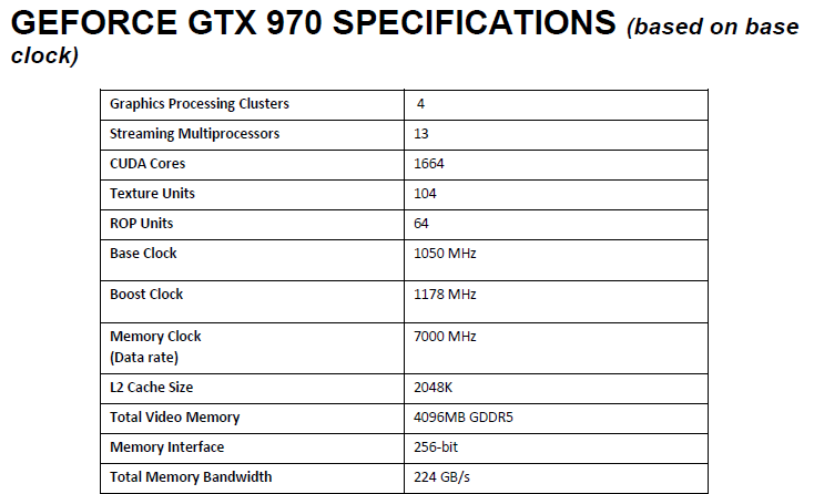
When the GTX 980 and GTX 970 were released, NVIDIA provided the above original specifications for the two cards. The launch GTX 900 GPUs would be a standard full/die-harvested card pair, with the GTX 980 using a fully enabled GM204 GPU, while the GTX 970 would be using a die-harvested GPU where one or more SMMs had failed. As a result of this the big differences between the GTX 980 and GTX 970 would be a minor clockspeed difference, the disabling of 3 (of 16) SMMs, and a resulting reduction in power consumption. Most important for the conversation at hand, we were told that both possessed identical memory subsystems: 4GB of 7GHz GDDR5 on a 256-bit bus, split amongst 4 ROP/memory controller partitions. All 4 partitions would be fully active on the GTX 970, with 2MB of L2 cache and 64 ROPs available.
This, as it turns out, was incorrect.
As part of our discussion with NVIDIA, they laid out the fact that the original published specifications for the GTX 970 were wrong, and as a result the “unusual” behavior that users had been seeing from the GTX 970 was in fact expected behavior for a card configured as the GTX 970 was. To get straight to the point then, NVIDIA’s original publication of the ROP/memory controller subsystem was wrong; GTX 970 has a 256-bit memory bus, but 1 of the 4 ROP/memory controller partitions was partially disabled, not fully enabled like we were originally told. As a result GTX 970 only has 56 of 64 ROPs and 1.75MB of 2MB of L2 cache enabled. The memory controllers themselves remain unchanged, with all four controllers active and driving 4GB of VRAM over a combined 256-bit memory bus.
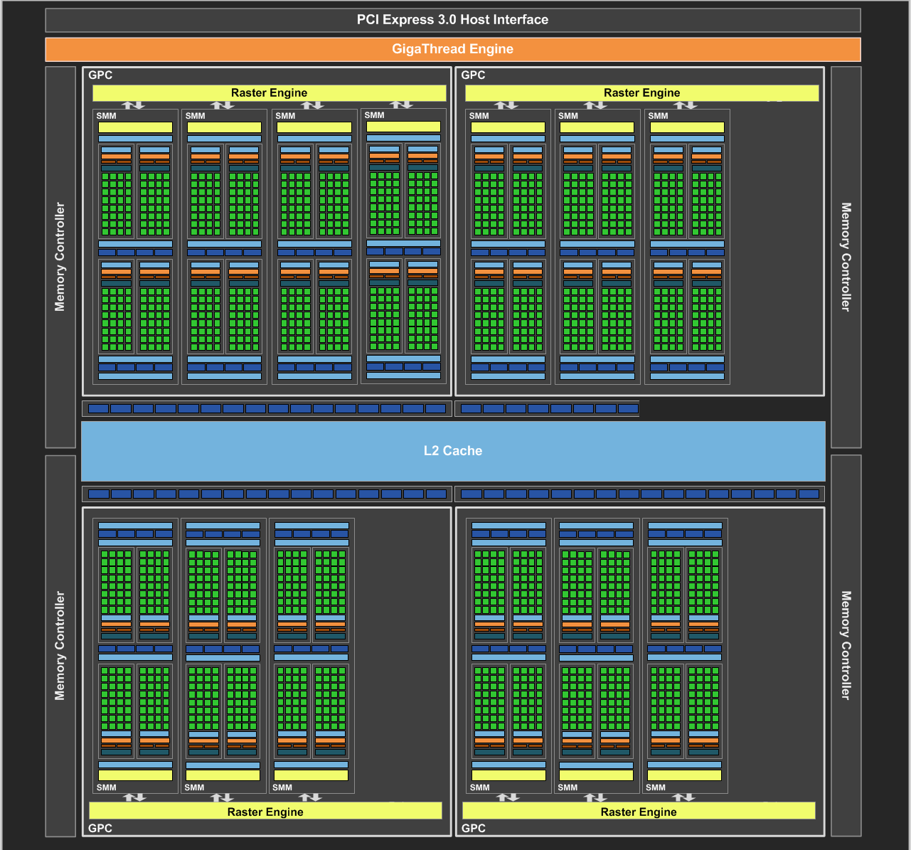
This revelation significantly alters how we perceive the performance of the GTX 970 in certain situations, and is the missing piece of the puzzle in understanding the memory allocation issues that originally brought all of this to light. The ability to “partially disable” a ROP/memory controller partition is new to Maxwell, and we’ll fully explore how that works in a moment, but the important part to take away is that the ROP/MC layout on the GTX 970 is not fully enabled like the GTX 980, and as a result will not behave identically to the GTX 980. All of the behavior from the GTX 970 we’ve seen in light of this correction now makes sense, and it is immediately clear that this is not a hardware or software bug in GTX 970, but rather the planned/intentional behavior of the product.
The biggest and most painful question about all of this then is how did this happen? How did we get fed incorrect specifications? NVIDIA’s explanation, in a nutshell, is that this was completely accidental and that all of this stems from assumptions made by NVIDIA’s technical marketing team.
GTX 970 Reviewer's Guide: Specifications
In short, while NVIDIA does publish the specifications of their cards on the GeForce website and in other places (e.g. partner product pages), those are less-detailed high level specifications suitable for a wider audience, not unlike NVIDIA’s initial statement. The deeper technical specifications we get, such as the number of ROPs, transistor count, and L2 cache size, comes from NVIDIA’s reviewer’s guide, which outlines for us the specifications of the card, the major new features that NVIDIA is focusing on, and some examples of benchmark numbers they’re seeing. This document is compiled by NVIDIA’s technical marketing team (a group no less than extensively knowledgeable about GPUs) based on the information provided to them by the product engineers and the product management team.
The error, as NVIDIA explains it, is that in creating the GTX 970 reviewer’s guide, the technical marketing team was unaware of Maxwell’s aforementioned and new “partial disable” capabilities when they filled out the GTX 970 specification table. They were aware that the GTX 970 would have the full 256-bit memory bus, and unaware of the ability to independently disable ROPs they assumed that all 64 ROPs and the full 2MB of L2 cache was similarly available and wrote the specification table accordingly. This error then made it into the final copy of the guide, not getting caught even after being shared around various groups at NVIDIA, with that information finally diffused by press such as ourselves.
Somewhat murkier is the intervening 4 months between the launch of the GTX 970 and the discovery of this error. As NVIDIA tell us, since the error wasn’t caught in the initial check of the reviewer’s guide there weren’t any further checks being made, especially since this information wasn’t also distributed via a public source (such as the GeForce website). As far as technical marketing knew the product had 64 ROPs, and as far as product management and engineering knew the technical marketing team had done their due diligence. As a result this issue was not caught and identified at NVIDIA until earlier this month when NVIDIA technical marketing started investigating the reports and requests from the press about the memory allocation oddities. Only after running similar tests and running into the same odd results as the press and users did NVIDIA properly identify the issue.
GTX 970 Memory Allocation (Image Courtesy error-id10t of Overclock.net Forums)
Now as NVIDIA is in full damage control mode at this point, consideration must be given as to whether NVIDIA’s story is at all true; NVIDIA would hardly be the first company to lie when painted into a corner by controversy. With that in mind, given the story that NVIDIA has provided, do we believe them? In short, yes we do.
To be blunt, if this was intentional then this would be an incredibly stupid plan, and NVIDIA as a company has not shown themselves to be that dumb. NVIDIA gains nothing by publishing an initially incorrect ROP count for the GTX 970, and if this information had been properly presented in the first place it would have been a footnote in an article extoling the virtues of the GTX 970, rather than the centerpiece of a full-on front page exposé. Furthermore if not by this memory allocation issues then other factors would have ultimately brought these incorrect specifications to light, so NVIDIA would have never been able to keep it under wraps for long if it was part of an intentional deception. Ultimately only NVIDIA can know the complete truth, but given what we’ve been presented we have no reason to doubt NVIDIA’s story.
In any case, going forward NVIDIA has made it clear that they intend to make sure this doesn’t happen again, to make sure that the specifications released to the press and public are better checked to ensure nothing is inaccurate or being assumed. NVIDIA rarely makes the same mistake twice, and certainly they will be under a great deal more scrutiny from here on to make sure their published specifications are correct.
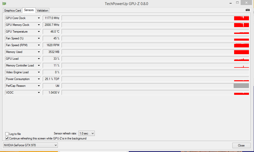
Meanwhile as press we play a role in this as well, as in retrospect we should have seen this sooner. Nebulous metrics such as VRAM allocation aside, NVIDIA’s own tools and our own experiences pointed to something being off. The pre-GM204 version of NVIDIA’s DeviceQuery CUDA application, for example, correctly reports that the GTX 970 only has 1.75MB of L2 cache and the GTX 980 has 2MB of L2 cache, even if it doesn’t fully understand the makeup of the Maxwell 2 architecture.
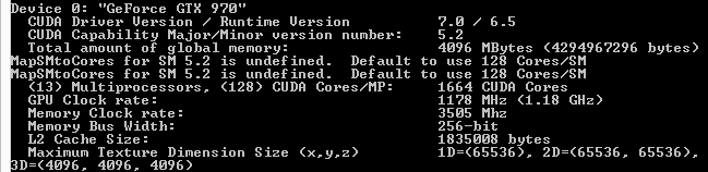
NVIDIA CUDA DeviceQuery: GTX 970
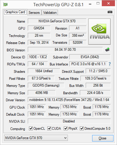
Furthermore our own initial incompatibility issues with the GTX 970 (and only the GTX 970) pointed to some kind of memory subsystem change that we should have looked into, even after NVIDIA corrected the problem in their drivers. Ultimately other tools such as GPU-Z and AIDA64 weren’t able to catch the difference since they too did not know about Maxwell’s ability to disable the ROPs, so only a limited number of flags were raised, but nonetheless this is something we admittedly should have been able to catch had we noticed what was wrong.


398 Comments
View All Comments
piiman - Saturday, January 31, 2015 - link
who cares how many transistors if it still runs great? This however impacts performance. Dying light turns into a stuttering mess the second the vram go over 3.5gb. This causes me to have to go from a surround 5670x1080 to a single screen and lower graphic settings overall at 1980x1080p , so I can stay under 3.5gb vram,to keep the game playing at an keep good FPS.The whole reason I bought 2 970s was to be able to play new 4k games as this could hurt that plan in a big way.
fonolavalencia - Wednesday, February 4, 2015 - link
Booooh, i have to play in one monitor, while people are dying in middle east !. you gringos will get the refound for sure, imagine myself being in ECUADOR... I hope they got a STEP UP program at least. This is very FISHY bussiness friends, we should stop this. And by the way, how about using an application to lower your ram to 3.5frodbonzi - Thursday, February 5, 2015 - link
Lol... this is a high end card, people dying in the Middle East have nothing to do with it, so get your trolling @ss out of here. And if you actaully bought 2 of these, you SHOULD NOT HAVE TO get an app to limit yourself to 3.5gb!! Especially if you bought them assuming they could handle 4gb!Morawka - Monday, January 26, 2015 - link
So what if they call everyone's bluff and offer refund's for the cards?that's what i would do if i were nvidia, just offer a refund, the majority of people will still keep their card, and nvidia could offer a free game to all those affected.
Then once the class action suit fires up, they can show all of the goodwill they offered and the case would lose serious steam.
spartaman64 - Monday, January 26, 2015 - link
i just hope nvidia updates the specs and put a disclaimer that there is .5GB of slow ramJlHADJOE - Tuesday, January 27, 2015 - link
Well, Nvidia's published specs (http://www.geforce.com/hardware/desktop-gpus/gefor... are technically correct, which some people would say is the best kind of correct.It's only the review sites really that posted stuff like ROP counts and cache size,
piiman - Saturday, January 31, 2015 - link
funny, they removed that link with the spec's. Perhaps they weren't that correct after all?fuckNvidia - Monday, February 9, 2015 - link
That was giving to them by nvidia, brainwash the public by the media and say we didn't say it, still is not right.xkieth - Thursday, January 29, 2015 - link
By majority of people, you mean, those people who bought 970 without any knowledge of the issue. nVidia gives them a free game out of the blue(from their perspective) and ofcourse, free game is free, accepts it, being the oblivious people that they are.then BAM!. Ubisoft 2.0
piiman - Saturday, January 31, 2015 - link
"So what if they call everyone's bluff and offer refund's for the cards?"A better solution is to turn on the ROP or offer 980's as replacements . Now that would be "good will"