NVIDIA Launches GeForce GTX 960
by Ryan Smith on January 22, 2015 9:00 AM EST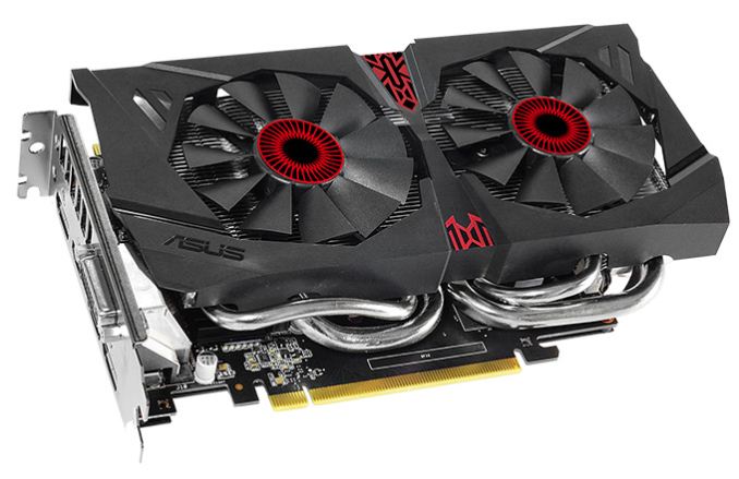
Editor's Note: Due to personal matters we won’t have a GeForce GTX 960 review published today. But in lieu of that we wanted to go over the basics of NVIDIA’s latest Maxwell card
With the launch of their first Maxwell GPUs just under a year ago, NVIDIA has by all accounts set themselves up on a solid trajectory for this generation of video cards. Maxwell has proven to be a sturdy GPU architecture, delivering strong performance alongside class-leading power efficiency. NVIDIA’s semi-refresh of Maxwell back in September for the “second generation” Maxwell GM2xx family (GTX 980 and GTX 970) served to further improve NVIDIA’s offerings, coupling Maxwell with a battery of new features for existing and future games alike.
So far we have seen NVIDIA release Maxwell into the low-end/mainstream market with the GTX 750 series, and then go after the high-end of the market with the GTX 980 and GTX 970. The last remaining piece of the puzzle for Maxwell is what comes between those two markets, the enthusiast market, typically served by NVIDIA’s x60 parts. Now just a bit over 4 months after NVIDIA’s launch into the high-end market, NVIDIA is back with their latest Maxwell GPU and latest video cards to do battle for the enthusiast market.
Launching today is the GeForce GTX 960 and the GM206 GPU. Following in the established traditions of the x60 video cards, NVIDIA is looking to reestablish their place in the enthusiast video card market with their latest offering. With GTX 980 and GTX 970 targeted at the 4K and 1440p markets, GTX 960 is in turn designed to be NVIDIA’s high-end 1080p card, capable of running most games with maximum (or near maximum) image quality at the still most common desktop resolution of 1920x1080. To do this they have brought down Maxwell 2 into GM206, a new, smaller GPU tailored for this market segment.
| NVIDIA GPU Specification Comparison | ||||||
| GTX 970 | GTX 960 | GTX 760 | GTX 660 | |||
| CUDA Cores | 1664 | 1024 | 1152 | 960 | ||
| Texture Units | 104 | 64 | 96 | 80 | ||
| ROPs | 56 | 32 | 32 | 24 | ||
| Core Clock | 1050MHz | 1126MHz | 980MHz | 980MHz | ||
| Boost Clock | 1178MHz | 1178MHz | 1033MHz | 1033MHz | ||
| Memory Clock | 7GHz GDDR5 | 7GHz GDDR5 | 6GHz GDDR5 | 6GHz GDDR5 | ||
| Memory Bus Width | 256-bit | 128-bit | 256-bit | 192-bit | ||
| VRAM | 4GB | 2GB | 2GB | 2GB | ||
| FP64 | 1/32 FP32 | 1/32 FP32 | 1/24 FP32 | 1/24 FP32 | ||
| TDP | 145W | 120W | 170W | 140W | ||
| GPU | GM204 | GM206 | GK104 | GK106 | ||
| Transistor Count | 5.2B | 2.94B | 3.5B | 2.54B | ||
| Manufacturing Process | TSMC 28nm | TSMC 28nm | TSMC 28nm | TSMC 28nm | ||
| Launch Date | 09/18/14 | 01/22/15 | 06/25/13 | 09/13/12 | ||
| Launch Price | $329 | $199 | $249 | $229 | ||
Starting off as always with the specs, it’s interesting to note just how very close GM206 comes to being half of a GM204. NVIDIA’s ‘6 parts being around half of a ‘4 is a common design goal for them, but in the last few generations it has never been quite so literal. GM206 and its GTX 960 launch partner feature half the shaders, half the memory bus, and half the ROPs, all at the same clockspeed. Since it is half of a GM204 though, this means that we’re looking at a fairly sizable gap between the GTX 960 and GTX 970; even with the latter’s disabled functional units, it’s still a much bigger, faster card than GTX 960, which reinforces the desired market segments for these cards.
At the heart of GM206 and GTX 960 is a Maxwell 2 configuration containing 1024 CUDA cores arranged in 8 SMMs over 2 GPCs, again reiterating the half-a-GM204 nature of the design. As this is a Maxwell 2 part this means NVIDIA’s CUDA core counts are essentially getting recalibrated here, as Maxwell’s per-core efficiency is well ahead of Kepler’s, leading to a “mere” 1024 CUDA cores punching well over their weight. On the other hand NVIDIA’s texture unit count is also down with the Maxwell generation, with texturing performance per unit being largely unchanged outside of some improvements to the cache feeding those units. On this matter NVIDIA believes Kepler was overweight on texturing, and in the case of GTX 980 and GTX 970 our performance figures haven’t shown Maxwell to be held back by this change.

Meanwhile GTX 960 is equipped with a relatively narrow and fast 128-bit memory bus. NVIDIA seems to be embracing 7GHz GDDR5 everywhere this generation, so even the GTX 960 gets top-speed GDDR5 this time around. With that said, the use of higher clockspeed GDDR5 also serves to in part offset that narrow memory bus, which at 128-bits wide is some 33% smaller than the 192-bit memory buses on GK106 and GF106. NVIDIA has never used a 128-bit bus on a ‘6 part before, and the fact that they’re doing so here certainly came as a shock at first.
With that said, as we discovered with GM204 Maxwell 2 introduces a new generation of color compression technology that in combination with caching improvements reduced memory bandwidth needs by around 25%. On GTX 980 and GTX 970 NVIDIA used this to significantly increase their effective memory bandwidth to efficiently drive 4K on a 256-bit memory bus, whereas on GTX 960 NVIDIA is essentially spending their gains on the narrower memory bus and ultimately a lower Bill of Materials (BoM). It goes without saying that NVIDIA has a great deal of faith in the real-world performance of their latest compression technology, as the 128-bit memory bus is here is practical thanks to it, but conversely only because of it.

Rounding out the major functional blocks on the GPU is a pair of ROP partitions, for 32 ROPs in total. This is consistent with Maxwell 2’s 16:1 ratio of ROPs to memory controllers, and overall keeps the number of ROPs equal with the outgoing GTX 760. Paired up with the ROPs is 1MB of L2 cache, which like virtually everything else is half the L2 of GM204, or significantly more than comparable Kepler parts.
From a theoretical performance perspective then, GTX 960 offers half the shading, texturing, ROP throughput, and memory bandwidth performance of NVIDIA’s flagship GTX 980. Or to make a more meaningful comparison, we’re looking at around 66% of the shading/texturing performance and 50% of the ROP/memory performance of GTX 970. Going the other direction is a bit more difficult due to architectural differences, but against the GTX 760 the GTX 960 offers 58% of the theoretical memory bandwidth and 102% of the shading performance, but again this is before accounting for the significant architectural gains. Which on that note, it’s always good to point out when discussing scaling up or down GPU architectures and performance does not scale up and down perfectly with functional unit counts, so while the GTX 960 trails the GTX 970 by quite a bit on paper, the GTX 970’s real world lead typically isn’t as great as the numbers would say.
On a feature note, while GM206 is officially classified as a Maxwell 2 part there is one small but very notable feature difference that needs to be pointed out, and we’ll get to in-depth in our full review. When it comes to HEVC (H.265) decoding, GM204, GM1xx, and GK1xx GPUs all offer limited HEVC decoding via a hybrid process that offloads some parts to the GPU fixed function units and shaders, and other parts to software entirely. However as of GM206 NVIDIA’s fixed function HEVC decoder has been completed and rolled into this GPU, making this the first discrete GPU with full HEVC decoding support. This will make the GTX 960 an especially tantalizing option for HTPC usage, but we’ll get deeper into that in the future.
GM206
Moving on, in keeping with the Maxwell tradition, GM206 continues to be a relatively sizable but very low power GPU. GM206 ends up weighing in at 2.94B transistors, 2.26B less than GM204 and 400M more than GK106. Like GM204 this has pushed the die size up compared to its predecessor, moving from GK106’s 214mm2 to GM206’s 227mm2. This is a smaller jump than GK104 to GM204, with GM206's die size ultimately being a combination of transistor savings from the narrowed memory bus along with a smaller jump in the number of CUDA cores and other functional units compared to GK106. The smaller jump in transistor count also offers a very crude hint that GM206 isn’t going to offer quite as big a performance increase over GK106 as GM204 offered over its predecessor. In other words, GM204 offered a lot more performance than GK104, but it was also quite a bit bigger. GM206 on the other hand isn’t much bigger than GK106, and performance expectations should be scaled accordingly.
As for power, with only 2.94B transistors GTX 960 is very easy on the power budget, coming in at a TDP of 120W, or a power target of 130W if looking at what the card is actually programmed to allow. This means that like GTX 660 before it, GTX 960 will be establishing itself as NVIDIA’s flagship sub-150W card, easily capable of being powered off of a single 6pin PCIe connector. At its performance level this also means that GTX 960 is going to deliver class-leading power efficiency, like the other Maxwell cards before it, though GTX 970 may end up holding on to the overall sweet spot of performance-per-watt in NVIDIA’s lineup. Otherwise by flipping once again from a ‘4 to a ‘6 GPU, NVIDIA’s power consumption compared to the GTX 760 is way down, as all of these first year product cycle Maxwell cards are riding the power efficiency sweet spot.
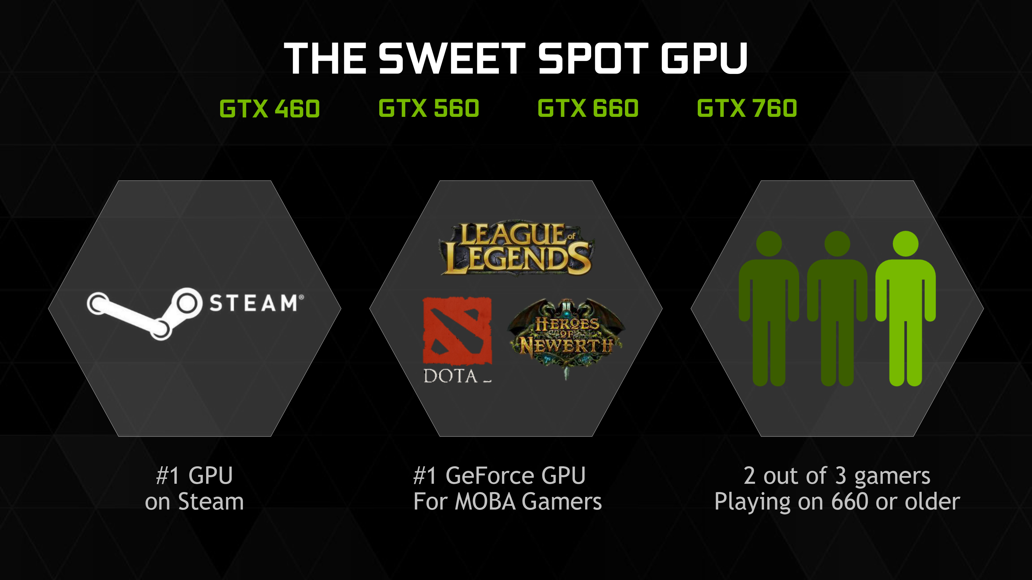
Overall NVIDIA is positioning the GTX 960 as their newest and greatest 1080p enthusiast class card, and the next upgrade for GTX 660/560/460 users. As we’ve discussed in prior articles NVIDIA is on roughly a 1 year product cycle but 2 year GPU cycle, so GTX 960 is not a significant step up from GTX 760 in performance, and consequently is not being pitched as an upgrade for current GTX 760 owners. NVIDIA tells us that they find that GTX x60 owners are typically on a 2-4 year upgrade cycle, which is fitting given the GPU generations in play and the reason why it’s primarily being pitched as a 660/560/460 replacement. To that end NVIDIA is touting just a 50% performance increase over GTX 660, with closer to a 2x increase in overall efficiency after factoring in the reduction in power consumption. One wildcard in any of these NVIDIA performance estimates is the use of MFAA as opposed to MSAA, which on that note NVIDIA tells us that they will be enabling MFAA for a much wider array of games. At this point NVIDIA is ready to enable it for more or less every game that doesn’t have a known problem with the AA technology, listing only 3 games with known issues: Dead Rising 3, Dragon Age 2, and Max Payne 3.


NVIDIA will be launching the GTX 960 at $199 MSRP, with today’s launch being a hard launch. There aren’t any reference card designs this time around, with NVIDIA’s partners launching customized cards right out of the gate. Not unlike the GTX 560 launch of a few years back, GTX 960’s overclocking prospects are looking very good, and as a result partners are launching with a large number of overclocked cards; in fact we’re seeing overclocked cards even at the $199 base price, and according to NVIDIA’s product list only 4 cards in the North American launch are shipping at the GTX 960’s base clockspeeds. It goes without saying then that so long as card pricing holds to MSRPs, there’s going to be little reason to grab a non-overclocked card on this launch. Particularly since these cards are also typically built for higher power targets, which offers headroom that may be useful in future overclocking.
Shifting gears to the competitive landscape, $199 is typically a hot market and the launch of the GTX 960 is no different. AMD’s competitors to the GTX 960 will be the Radeon R9 285 and the Radeon R9 280, the latter of which is something of a story in and of itself, having stubbornly refused to take up its planned retirement after the launch of the 285. With prices of the 280 in particular typically below $199 we have an unusual situation where AMD and partners are unloading 3GB Tahiti cards for relatively little, which will keep this from being an easy win for NVIDIA like GTX 980/970 were. With that said, this is otherwise setting up to be a repeat of the aforementioned launch, with AMD able to compete with NVIDIA on price/performance but not Maxwell’s power efficiency.
Finally, it’s worth noting that there are no game bundles in play at this time for either side. So for the launch of the GTX 960 everything will be a straightforward value proposition.
| Winter 2015 GPU Pricing Comparison | |||||
| AMD | Price | NVIDIA | |||
| Radeon R9 290X | $330 | GeForce GTX 970 | |||
| Radeon R9 290 | $270 | ||||
| Radeon R9 280X | $230 | ||||
| Radeon R9 285 | $200 | GeForce GTX 960 | |||
| Radeon R9 280 | $180 | ||||
Anyhow, that’s a wrap from us for now. Be sure to check back in early next week for our complete look at GeForce GTX 960, including performance, overclocking, HEVC support, and more.


87 Comments
View All Comments
rocktober13 - Thursday, January 22, 2015 - link
I'm disappointed not to see any reference card designs. With HEVC support and low TDP, the 960 is perfect for my mini-ITX HTPC, but I think it needs to exhaust it's own heat in order to keep the rest of the components cool.Samus - Thursday, January 22, 2015 - link
Hopefully someone just smacks a reference 750Ti cooler on it. Perfect ITX size and the cooler is probably capable of cooling a 120-watt TDP chip with some material and surface area tweaking.kwrzesien - Thursday, January 22, 2015 - link
Check the gallery - it looks like MSI is selling a blower version.VeauX - Thursday, January 22, 2015 - link
For HTPC I was looking more into a low profile card. And it happens that the most recent performing one is the 750 ti... Hard to put a hand on though ... If a LP 660 comes out this would definitely be an appeal to meMrSpadge - Thursday, January 22, 2015 - link
Ryan, when you do the full review can you poke nVidia whether the delta color compression also applies to GP-GPU loads?The reason I'm asking is that we see even GTX970, which has more bandwidth per shader than other Maxwells, to be severely limited by memory bandwidth under some BOINC projects. Einstein@Home runs at ~75% memory controller load and a well-configured SETI@Home at 100%. Both projects are looking for patterns in signals which contain mostly random noise, so there's probably nothing to compress.
Making things even worse for GM204 is that under GP-GPU load (CUDA or OpenCL) the card is only allowed to run at performance level P2, where the memory is clocked at 6.0 GHz instead of 7.0 GHz. Try it: run e.g. Heaven in windowed mode and everything is fine. Then launch a GP-GPU program (e.g. memtestCL) along with it and memory clock & p-state drop immediately. nVidia inspector can show this. It can also increase the memory clock under P2 (which other utilities can't), but it's cumbersome because the GPU must not be running any GP-GPU work for the changes to have any effect. Also P2 memory clock can't be set higher than P0, so you always have to adjust both.
Watch out for these errors (eh, "unwanted behaviour") on GM206!
Ktracho - Thursday, January 22, 2015 - link
When you run GPGPU applications, would you rather get fast results, or more assurance that your results are correct? Overclocking is not a friend of correctness, which is why NVIDIA's Tesla cards are never clocked as fast as their desktop graphics cards. In that sense, I think some gratefulness is warranted, in that if GM204 cards did not slow down when running GPGPU applications, but instead occasionally made mistakes in their calculations, then you'd have to go and manually slow down your card every time you wanted to run such applications.MrSpadge - Friday, January 23, 2015 - link
I'm not talking about overclocking, I'm talking about reaching the stock memory clock. The one the chips are being sold for, and the clock which is being advertised. If this was a matter of calculation errors, neither company should be allowed to sell the products like this (and the gamers would see more graphics errors & artifacts). And some Keplers ran GP-GPU just fine with 7.0 GHz stock memory clocks.Ryan Smith - Thursday, January 22, 2015 - link
Delta color compression does not apply to GPGPU workloads. It only applies to graphics worksloads.Parablooper - Thursday, January 22, 2015 - link
Really interesting picture about the GTX -60 series! Didn't know it was so predominant.xrror - Friday, January 23, 2015 - link
So my oldschool "get off my lawn" comment is as follows...The benches are in, and GTX 960 sucks for a $200 card. And honestly it follow the footsteps of the 750 750/ti that also sucked (but everyone blushed about how power efficient it was, meh).
Okay, so before you label me an nVidia troll, my anger isn't for the reasons you think.
nVidia has mastered the art of stopping people from overclocking via limiting TDP. Hard. This sucks.
You'll never see a 970 beat a 980, or 960 be decent because before you could ever overclock enough nVidia will yank you back.
The 750 and 750ti also were gimped like this.
So my anger is yea, welcome to the new age of hardware enforced market segmentation. IN THE OLD DAYS if the GTX 960 was released, it would have been more exciting to see what more daring OEMs and/or overclockers did with this "salvaged" GPU die. GTX 960 @ 2.0GHz+ would have been interesting, and at least worth your time to look at.
Like say, overclocked GTX760 cards were at least interesting (Also note now nVidia NEVER released the card everyone wanted - GTX760ti). But GTX 960? Not even OEMs can get anything fun out of it.
So yea, welcome to the new world of hardware enforced Market Segmentation. It's been coming for a while, and we've seen the dust on the horizon for a few years now - it just happens that the GTX 960 is the product that really epitomizes it for graphics cards.
Yea, Intel has done this for years now, but at least they throw us a bone. (Don't believe me? Try overclocking P43 chipset over 420mhz - and that's ancient history now. Intel knows how to limit clock in hardware, they've just not completely shut you out.... yet).