NVIDIA Tegra X1 Preview & Architecture Analysis
by Joshua Ho & Ryan Smith on January 5, 2015 1:00 AM EST- Posted in
- SoCs
- Arm
- Project Denver
- Mobile
- 20nm
- GPUs
- Tablets
- NVIDIA
- Cortex A57
- Tegra X1
GPU Performance Benchmarks
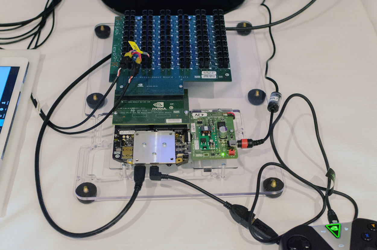
As part of today’s announcement of the Tegra X1, NVIDIA also gave us a short opportunity to benchmark the X1 reference platform under controlled circumstances. In this case NVIDIA had several reference platforms plugged in and running, pre-loaded with various benchmark applications. The reference platforms themselves had a simple heatspreader mounted on them, intended to replicate the ~5W heat dissipation capabilities of a tablet.
The purpose of this demonstration was two-fold. First to showcase that X1 was up and running and capable of NVIDIA’s promised features. The second reason was to showcase the strong GPU performance of the platform. Meanwhile NVIDIA also had an iPad Air 2 on hand for power testing, running Apple’s latest and greatest SoC, the A8X. NVIDIA has made it clear that they consider Apple the SoC manufacturer to beat right now, as A8X’s PowerVR GX6850 GPU is the fastest among the currently shipping SoCs.
It goes without saying that the results should be taken with an appropriate grain of salt until we can get Tegra X1 back to our labs. However we have seen all of the testing first-hand and as best as we can tell NVIDIA’s tests were sincere.
| NVIDIA Tegra X1 Controlled Benchmarks | |||||
| Benchmark | A8X (AT) | K1 (AT) | X1 (NV) | ||
| BaseMark X 1.1 Dunes (Offscreen) | 40.2fps | 36.3fps | 56.9fps | ||
| 3DMark 1.2 Unlimited (Graphics Score) | 31781 | 36688 | 58448 | ||
| GFXBench 3.0 Manhattan 1080p (Offscreen) | 32.6fps | 31.7fps | 63.6fps | ||
For benchmarking NVIDIA had BaseMark X 1.1, 3DMark Unlimited 1.2 and GFXBench 3.0 up and running. Our X1 numbers come from the benchmarks we ran as part of NVIDIA’s controlled test, meanwhile the A8X and K1 numbers come from our Mobile Bench.
NVIDIA’s stated goal with X1 is to (roughly) double K1’s GPU performance, and while these controlled benchmarks for the most part don’t make it quite that far, X1 is still a significant improvement over K1. NVIDIA does meet their goal under Manhattan, where performance is almost exactly doubled, meanwhile 3DMark and BaseMark X increased by 59% and 56% respectively.
Finally, for power testing NVIDIA had an X1 reference platform and an iPad Air 2 rigged to measure the power consumption from the devices’ respective GPU power rails. The purpose of this test was to showcase that thanks to X1’s energy optimizations that X1 is capable of delivering the same GPU performance as the A8X GPU while drawing significantly less power; in other words that X1’s GPU is more efficient than A8X’s GX6850. Now to be clear here these are just GPU power measurements and not total platform power measurements, so this won’t account for CPU differences (e.g. A57 versus Enhanced Cyclone) or the power impact of LPDDR4.
Top: Tegra X1 Reference Platform. Bottom: iPad Air 2
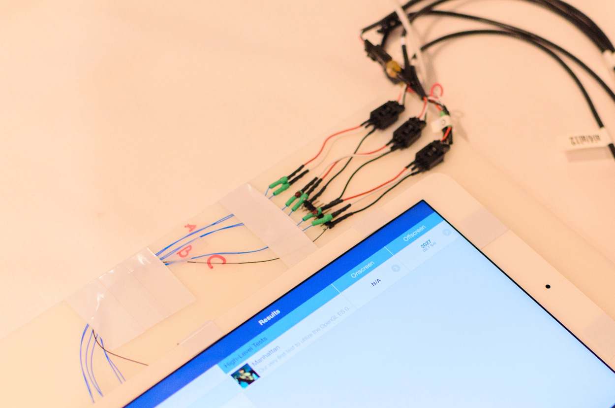
For power testing NVIDIA ran Manhattan 1080p (offscreen) with X1’s GPU underclocked to match the performance of the A8X at roughly 33fps. Pictured below are the average power consumption (in watts) for the X1 and A8X respectively.
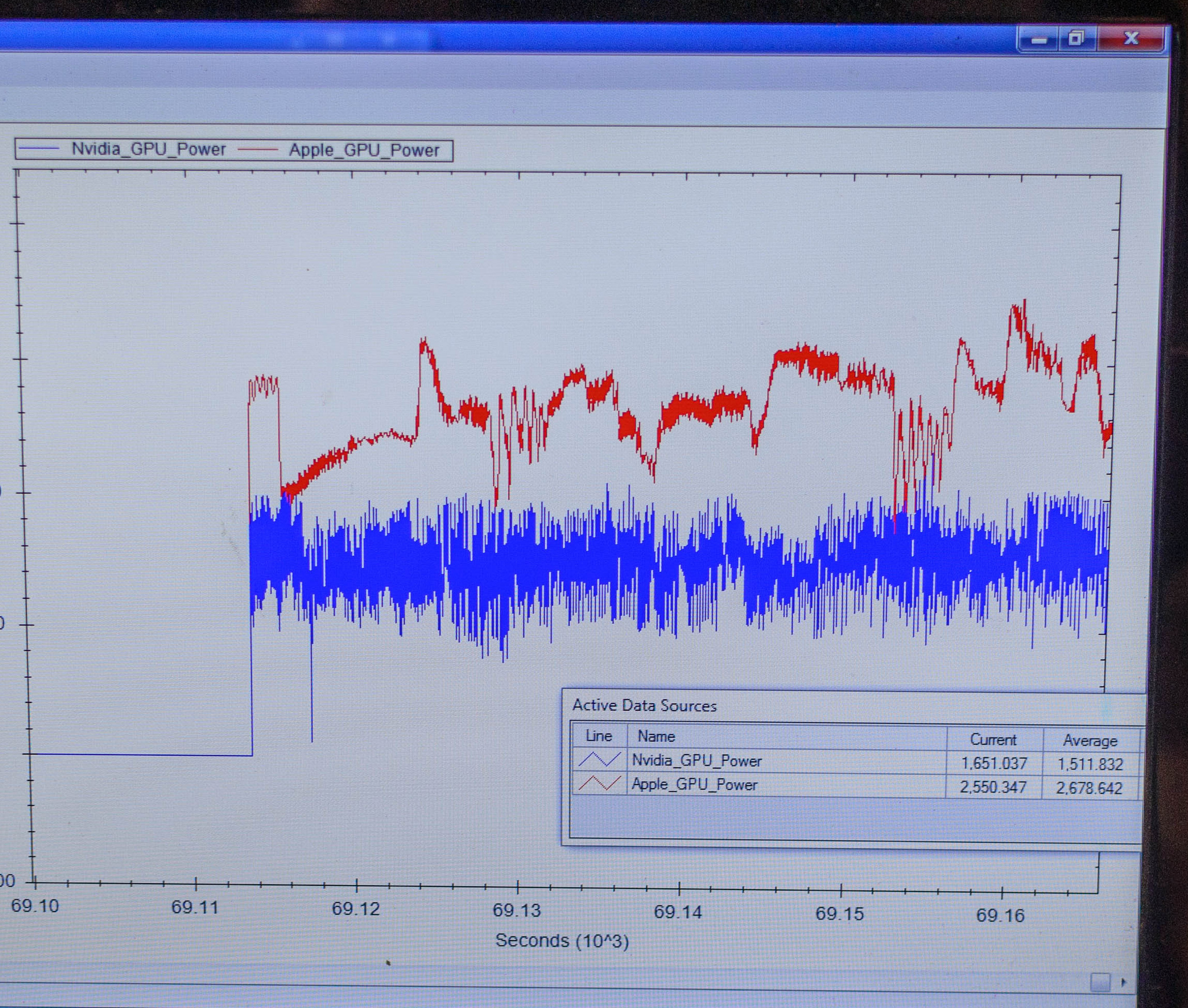

NVIDIA’s tools show the X1’s GPU averages 1.51W over the run of Manhattan. Meanwhile the A8X’s GPU averages 2.67W, over a watt more for otherwise equal performance. This test is especially notable since both SoCs are manufactured on the same TSMC 20nm SoC process, which means that any performance differences between the two devices are solely a function of energy efficiency.
There are a number of other variables we’ll ultimately need to take into account here, including clockspeeds, relative die area of the GPU, and total platform power consumption. But assuming NVIDIA’s numbers hold up in final devices, X1’s GPU is looking very good out of the gate – at least when tuned for power over performance.


194 Comments
View All Comments
SM123456 - Sunday, February 1, 2015 - link
>>He was saying: why NV didn't continue with Denver design? Being so efficient and only 2 cores why don't shift at 20nn easily? Because they can't and that's it. The other things are speculations.<<There is a simple answer to that - Apple has booked all the production slots for 20nm (made by foundry TSMC) to meet demand for the A8. This has pushed back production of the 16nm to late 2015. That is the reason for the delay in Denver, which nVidia originally intended for the Tegra K1 Denver successor, the Pascal chip. That is the reason for the delay in Pascal.
20nm is a risk reducing interim technology which almost everybody is skipping. Apple originally wanted 14/16nm for the A8, only used 20nm because they couldn't wait to release the current iPhone on 14/16nm. nVidia is only producing the Tegra X1 at 20nm because they are worried about the same problem happening at 16nm. With 20nm, they know that Apple will be moving off 20nm with the next iPhone, so there will definitely be spare production capacity.
utferris - Monday, April 13, 2015 - link
I can not agree you any more. They aliens can not be reasonable.GC2:CS - Wednesday, January 7, 2015 - link
2) I could make 4 cluster A7 GPU faster than tegra K1 and I could make a 16 cluster series 7XT GPU that's slower than tegra K1.So tell me how the heck does the number of clusters or "cores" relates to efficiency ???
lucam - Wednesday, January 7, 2015 - link
Since you re so expert about Imagt cluster you can explain why there some model of G6230 - 2 clusters (Allwinner socs) fast as much as an A7 (G6430) - 4 clusters. Maybe because the former has clock frequency higher than latter? But are pretty much the same in term of performance/watt....there we go..SM123456 - Sunday, February 1, 2015 - link
Errr.. same performance and price per watt for Apple on 20nm as nVidia at 28nm? That is damning.SM123456 - Sunday, February 1, 2015 - link
The cores aren't important, the performance is. That is the whole point. The responsiveness depends on single core performance and to a lesser extent two core performance, and on this point Denver beats the crap out of the Apple A8 and A8X. Therefore the fact that Apple added an extra core to the A8 to get A8X is about benchmark bragging rights, and the A8X real world performance (based on single and dual core performance) lags the Tegra K1 Denver even with A8X on 20nm and Denver K1 on 28nm - not good for Apple.lucam - Tuesday, January 6, 2015 - link
The Tegra speculations of chizow are priceless!aenews - Saturday, January 24, 2015 - link
The K1 is four months or so older than the A8X. It crushed every chip very badly for four whole months. If anything, everyone else was/is playing catchup. And not to mention the Snapdragon 810, yet to be released, does not even come close to the K1 despite being a year newer.utferris - Monday, April 13, 2015 - link
> "The K1 is four months or so older than the A8X."How do you come up with that?
A8X was in production way before K1.
It is just you see A8X only on ipad, when NVidia is showing off all around the test board that does not actually in production.
chizow - Monday, January 5, 2015 - link
@Mayuyu; I wouldn't be surprised if this is the final outcome of the Nvidia IP Patent lawsuits and why Apple was excluded from the original litigation. My bet is they (Apple) have already engaged in serious talks with Nvidia and they are both just awaiting a favorable outcome against Samsung/Qualcomm before moving forward.