ARM A53/A57/T760 investigated - Samsung Galaxy Note 4 Exynos Review
by Andrei Frumusanu & Ryan Smith on February 10, 2015 7:30 AM ESTCortex A53 - Architecture
As the owners and creators of the ARM instruction set architecture, ARM (the company) is in an interesting place with regards to both CPU and ISA development. Unlike any other ISA architect, ARM both designs CPUs off of their ISA and licenses that ISA out to other companies as well, creating a marketplace where ARM is both a master and a competitor all at once. From a financial perspective ARM wins either way – architecture licensees pay royalties as well as CPU licensees – but it means that ARM’s CPU designs are by no means a shoe-in, especially at the lucrative high-end of the market.
At the same time the forward-looking nature of ARM’s licensing business means that we get to see their hand well before anyone else’s, as ARM’s licensing model is based around announcing their in-house Cortex CPU designs years in advance to attract customers. Quite often we will know what ARM’s CPU designs are months (or years) before we know what their competition will be. Case in point, for ARMv8 ARM announced their Cortex A53 and Cortex A57 designs over 2 years ago, meaning that although the A53 and A57 product designations are well known, it’s only now that we truly get to see the fruits of ARM’s labor in the consumer market.
At the small end of ARM’s ARMv8 processor lineup is the A53. The successor to the A7, the A53 embodies the same incredibly low power, small die size, and moderate performance goals of the A7 while extending the architecture to 64-bits, as well as working in some further performance improvements. A7 was popular on its own in lower-end Android devices, and for A53 we expect the situation to be much the same. However for the purpose of Exynos, its calling will be as the LITTLE half of its big.LITTLE configuration to drive the SoC during low-performance circumstances.

As with A7, A53 is an in-order design, which in some ways makes it the more interesting of the two ARMv8 designs out of ARM. While A57 gets a comparatively huge die size and power budget to implement high performance features, A53 gets little power, little die size, and ultimately has to get whatever performance it can out of in-order execution. With out-of-order execution being prohibitively expensive in die space and power for A53, this puts ARM in the position of trying to optimize an in-order design as far as they can, explicitly without making the jump to Out-of-Order Execution (OoOE).
Peter Greenhalgh, lead architect of the A53, had a few words to say on the design goals of A53 while taking questions as a guest late last year in a Q&A session here at AnandTech:
Cortex-A53 has the same pipeline length as Cortex-A7 so I would expect to see similar frequencies when implemented on the same process geometry. Within the same pipeline length the design team focused on increasing dual-issue, in-order performance as far as we possibly could. This involved symmetric dual-issue of most of the instruction set, more forwarding paths in the data-paths, reduced issue latency, larger and more associative TLB, vastly increased conditional and indirect branch prediction resources, and expanded instruction and data prefetching. The result of all these changes is an increase in SPECInt-2000 performance from 0.35-SPEC/MHz on Cortex-A7 to 0.50-SPEC/MHz on Cortex-A53. This should provide a noticeable performance uplift on the next generation of smartphones using Cortex-A53.
At its core, the A53 retains the same execution characteristics of the A7. This means we’re looking at a dual-issue in-order CPU with a nice and short 8-stage pipeline. This is coupled with a variable amount of both L1 data cache and L1 instruction cache, ranging from 8KB to 64KB each. L2 cache meanwhile is optional and similarly variable from 128KB to 2MB – Exynos 5433 uses 512KB 256K of the stuff – with there being a single, wide interface between the entire collection of A53 cores and the L2 cache, allowing each core to access the L2 in sequence.
| ARM CPU Core Comparison | ||||||
| Cortex-A7 | Cortex-A53 | |||||
| ARM ISA | ARMv7 (32-bit) | ARMv8 (32/64-bit) | ||||
| Issue Width | 2 micro-ops | 2 micro-ops | ||||
| Pipeline Length | 8 | 8 | ||||
| Integer Add | 2 | 2 | ||||
| Integer Mul | 1 | 1 | ||||
| Load/Store Units | 1 | 1 | ||||
| Branch Units | 1 | 1 | ||||
| FP/NEON ALUs | 1x64-bit | 1x64-bit | ||||
| L1 Cache | 8KB-64KB I$ + 8KB-64KB D$ | 8KB-64KB I$ + 8KB-64KB D$ | ||||
| L2 Cache | 128KB - 1MB (Optional) | 128KB - 2MB (Optional) | ||||
For A53, ARM has opted to focus on improving the processor at every stage in order to improve the performance of its dual-issue design. Of these changes, the biggest changes are in the dual-issue capabilities of the processor itself, along with changes to branch prediction.
In the case of dual-issue capabilities, ARM has increased the types of operations that can be issued from the second instruction slot, slot-1. With A7 slot-0 was full-featured while slot-1 could only issue branch and integer data; now for A53, slot-1 can also issue load-stores and FP/NEON operations, bringing it up to parity with slot-0. This means that as far as dual-issue conditions go, A53 should now only be limited by available execution units and whether the next operation can safely be co-issued.
Meanwhile for branch prediction, ARM has worked on beefing up A53’s branch unit to improve the hit rate and otherwise reduce the time wasted on mispredicted branches. Here A53 gains new conditional and indirect predictors, with the conditional predictor being a 6Kbit gshare predictor, while the indirect predictor can hold 256-entries with path history.
Elsewhere, when it comes to power, the A53 has an optional new ability to better switch between power states. The new architecture adds new retention states that are able to power-gate individual blocks of the CPU core, such as for example the NEON unit, and provide lower latency power-gating idle states.
As far as performance goes, ARM tells us that A53 can match A9 in performance at equivalent clock speeds. Given just how fast A9 is and just how small A53 is, to be able to match A9’s performance while undercutting it in die size and power consumption in this manner would be a feather in ARM’s cap, and an impressive follow-up to the A8-like performance of A7.
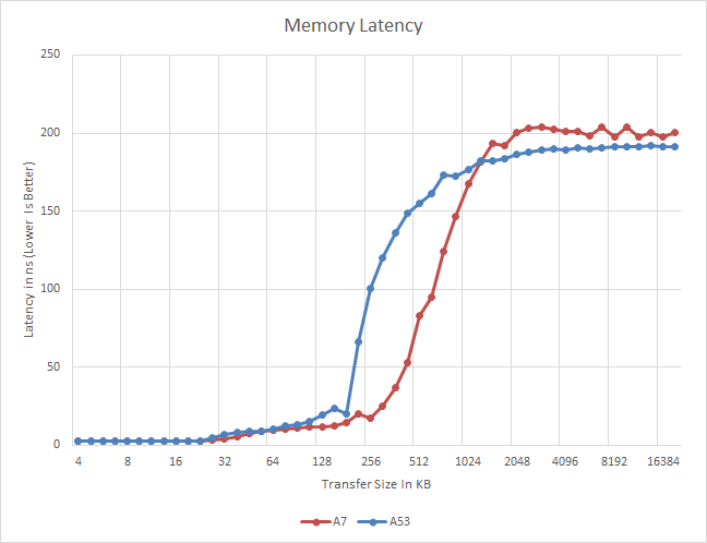
Meanwhile a quick look at some of our synthetic tests finds that the A53 cores in the Exynos 5433 are doing unusually poorly in latency compared the A7 cores, despite the fact that both parts have 512KB 256K of L2 cache. We have other reasons to believe the 5433 has 512KB of L2 cache for the A53 cores,* but looking at this you wouldn't think so, as latency shoots up much earlier, making it seem as if the chip has only 256KB of cache.
* Correction 24/03/2015: Our initial info of 512K L2 cache on the A53 cluster was incorrect and has henceforth been edited to 256K as published by Samsung. (Source)
Given the new information, it looks like the A53 is behaving as it should and the anomaly we saw in the data is actually a proper representation of the real-world scenario.
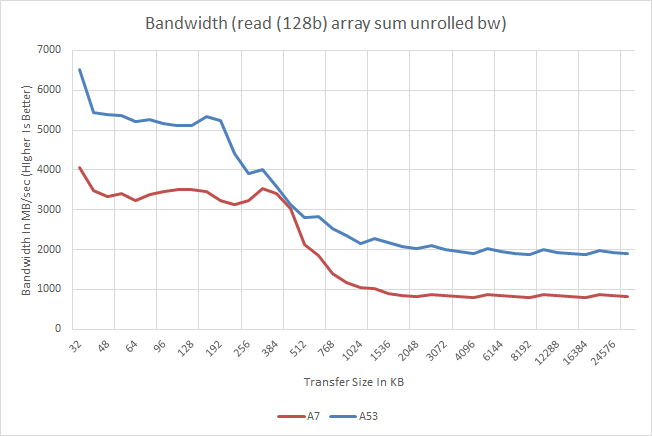
Switching from latency to read bandwidth, we find an interesting outcome for the A53 in the Exynos 5433: memory bandwidth, a lot of it. Truth be told I'm still scratching my head at this one; it's not clear whether this is a result of the dual-issue improvements, something Samsung did for 5433, both, or something else entirely. But the A53 cores in the 5433 have roughly twice as much memory bandwidth as the A7 cores in 5430. This is the case both inside the cache areas and outside to main memory, which points to some greater factor at work here.
Finally, it’s interesting to note at this point that after taking care of the dual-issue bottlenecks on A53, ARM has come very close to pushing a dual-issue in-order design as far as they can go. With most instructions executing in 1 cycle, A53 executes as wide a variety of instructions as quickly as it can, and consequently improving branch prediction is one of the few avenues left for further improving performance. This may partially explain why ARM has already announced the A57’s successor for a couple of years down the line – A72 – but has not announced an A53 successor. Short of going wider or OoOE, I would be curious to see what ARM does after A53.


135 Comments
View All Comments
DarkLeviathan - Saturday, December 19, 2015 - link
They added another core in the new iPad for a totally different reason. Its like having a laptop and a desktop.And there are several reasons why having dual cores in the iPhone is better and having dual cores in the iPad would be a worse idea.
1. The cores in the iPad would get so big and inefficient that it would be pointless to make them bigger. The battery would be wasted. However on the iPhone, the 2 cores are the best size as it is not too small to be slow and too big to be too power hungry.
2. The 3 cores on the iPad is there because they have more space. If they went full Samsun retard style with 4 or 8 cores, you would see 4 or 8 cores with high clock speeds but very low processing power. And therefore inefficient wast of resources and space. Not to mention that most apps only use 1 or 2 cores to run.
zepi - Tuesday, February 10, 2015 - link
Outstanding article, once again.Only thing I'm worried is that writes of such pieces are "Hot Shit" in employment market and I fear our technical writers could yet again disappear to better paying tech-companies...
Andrei Frumusanu - Tuesday, February 10, 2015 - link
I don't plan on going anywhere for the foreseeable future :)Ryan Smith - Tuesday, February 10, 2015 - link
Indeed. Better leg shackles have proven to be an excellent investment this year.rd_nest - Tuesday, February 10, 2015 - link
Wonderful article, loved the detailed analysis done. I wonder if there are any improvements in software stack in 7420 compared to 5433 specially since 7420 will be shipped worldwide.Andrei Frumusanu - Tuesday, February 10, 2015 - link
I'm looking forward to analysing those changes. There should be a considerable amount of change given the new AArch64 kernel platform, but we won't know till it's out.arayoflight - Tuesday, February 10, 2015 - link
I hope to see such an article again in future for the Exynos 7420. Just don't delay that this much.hlovatt - Tuesday, February 10, 2015 - link
I would second zepi's comment "outstanding article", shows why AnandTech is still way ahead of other review sites.TomWomack - Tuesday, February 10, 2015 - link
I'm really impressed by some of the fiddly things you've managed to measure here. What was your source for the die area measurements (Chipworks hasn't done a 5433 tear-down yet), and did you set up the detailed power-monitoring hardware yourself?Andrei Frumusanu - Tuesday, February 10, 2015 - link
The power measurement setup is my own work and we'll hopefully see more of it in the future.