Apple Announces A8 SoC
by Ryan Smith on September 9, 2014 1:45 PM EST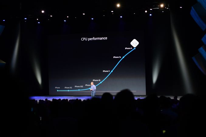
As expected from this year’s iPhone keynote, Apple has announced a new member of their internally developed family of ARM SoCs.
The latest SoC, dubbed A8, is Apple’s first SoC built on the 20nm process, and among the first SoCs overall to be built on this process. Apple notes that it has 2 billion transistors and is 13% smaller than the A7, which would give it upwards of twice as many transistors as the A7 and would put the die size at about 89mm2.
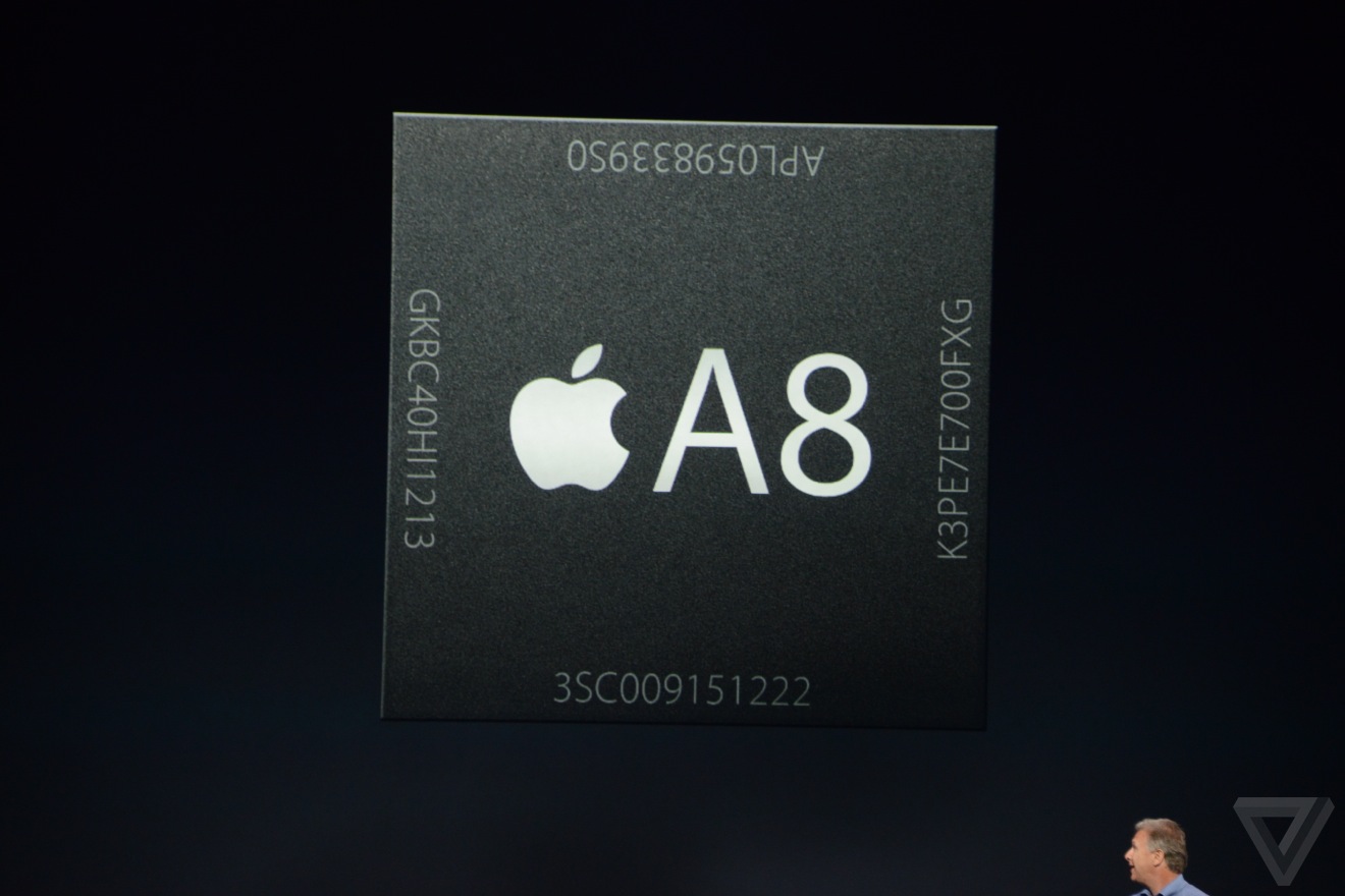
Image courtesy The Verge
From a performance perspective Apple is promising 25% faster CPU performance than A7. As is usually the case with Apple, they aren’t talking about the underlying CPU core – though this is a problem we’re working to rectify – so it remains to be seen how much of this is due to CPU architectural upgrades and how much is from clockspeed improvements afforded by the 20nm process. Apple just introduced their 64bit Cyclone core last year, so it stands to reason that just a year later and with the transition to 64bit already completed, A8 packs a CPU that is similar to Cyclone.
| Apple SoC Evolution | |||||
| CPU Perf | GPU Perf | Die Size | Transistors | Process | |
| A5 | ~13x | ~20x | 122m2 | <1B | 45nm |
| A6 | ~26x | ~34x | 97mm2 | <1B | 32nm |
| A7 | 40x | 56x | 102mm2 | >1B | 28nm |
| A8 | 50x | 84x | 89mm2 | ~2B | 20nm |
Meanwhile Apple is being even less specific about the GPU, but from their published baseline performance comparisons against the iPhone 1, the A8 is said to be 84x faster on graphics. This compares to a published figure of 56x for the A7, which implies that the A8’s GPU is 1.5x faster than the A7’s. Given Apple’s conservative stance on clockspeeds for power purposes and the die space gains from the 20nm process, it seems likely that Apple has upgraded from a 4 core PowerVR GPU to a 6 core PowerVR GPU, likely the flagship GX6650, which would account for the 50% performance gain right there.
Finally, Apple notes that the A8 is designed to be 50% more energy efficient than the A7. Some of these efficiency gains would come from gains due the 20nm process, however this large of a gain would indicate that Apple has done additional work at the architectural level to improve efficiency, as smaller manufacturing nodes alone do not see these kinds of gains.
Update: We have posted our initial A8 analysis here


66 Comments
View All Comments
ancientarcher - Wednesday, September 10, 2014 - link
Just stop acting like the Intel shill that you areIntel core M had 1.3bn transistors and an area of 82 sqmm. So, 1.6bn xtors per 100sqmm
Apple A8 has 2bn xtors and an area of 89 sqmm. So, 2.25bn xtors per 100 sq mm
Those numbers are not even in the same ball park. The xtor density that TSMC 20nm offers is much better than Intel's so called 14nm. Or is that still in doubt because you posted a link to some marketing slide from Intel??
witeken - Wednesday, September 10, 2014 - link
Okay, here are some facts:-28nm and 22nm have about the same density
-14nm has a 2.2X higher density than 22nm
-20nm has a 1.9X higher density than 28nm (those numbers are theoretical limits)
According to your calculation, that would mean that 20nm somehow manages to get a 3.1X increase in density as opposed to the realistic 1.9X, which nicely fits in Moore's Law.
So I wouldn't buy too much into Apple marketing talk.
DERSS - Saturday, September 13, 2014 - link
A8 is SOC that has 2 GB RAM in it as separate crystal that is layered over CPU-GPU one.witeken - Wednesday, September 10, 2014 - link
Actually, you could be right. The reason being that Apple's A8 SoC is optimized for density (most of the SoC doesn't have to run at high frequencies and the CPU is only a small fraction of the die), while Broadwell uses transistors optimized for performance and power, because it has to run a up to 2.6GHz.So this is not an apples to apples comparison. You'd have to compare *at least* Cherry Trail with A8 to get a fair comparison. Those should be about equal.
melgross - Tuesday, September 9, 2014 - link
The clock is just about the same. Last year it was 1.3GHz, and now it's 1.4GHz. That's almost nothing.name99 - Tuesday, September 9, 2014 - link
Where did that 1.4GHz figure come from?Remember Apple's goal is not to win some dick-measuring contest, it's to provide what they consider to be the best balance between
- snappy (peak) performance
- sustained performance
- battery life
Going forward their best bet is probably to follow the Intel track as much as possible, meaning they stick with this sort of low frequency but keep providing better and better turbo.
name99 - Tuesday, September 9, 2014 - link
Another possibility (something Apple hasn't done that much yet but could going forward) is to be much more aggressive with binning.We could have something like the 6+ getting 100MHz faster CPU than the 6, and the mythical iPad Pro (or iPad+???) getting the very fastest chips that can be binned. That way Apple can shut up some of the criticism of "slow frequencies" by shipping some devices that are running at 1.8MHz or whatever.
Alexey291 - Thursday, September 11, 2014 - link
and there was me thinking that apple's goal was to earn the largest profit possible. But it turns out that they are this altruistic entity doing the best they can for their customers....Gondalf - Tuesday, September 9, 2014 - link
Core M die is the same of standard Broadwell U 2+2 and these SKUs must clock at well over 3Ghz Turbo.Obviously a fast SKU is less denser than a low/medium perf SOC, at least i hope you know this........
name99 - Tuesday, September 9, 2014 - link
A8 refers to the *SoC*. THAT has twice as many transistors.Where do the extra transistors go?
Probably quite a few went to the h.265 engines. (Those APPEAR to be part of the system though they were not called out in the keynote. They are referred to in the iPhone6 FaceTime sections on apple.com. My theory is that Apple had a grand plan for announcing h.265 support everywhere simultaneous with 4K movie support and retina iMacs and MBAs. The Broadwell delay has sunk those plans, so the h.265 support will be there, but unpublicized for a while.)
Likewise improved ISP.
I also suspect (hope!) that the focus of the A8 CPU redesign was the uncore not the core. This is what I suggested a few weeks ago --- the core is basically unchanged except manufactured in 20nm and so faster [and perhaps various circuit tweaks for power] --- but the uncore (L2, L3 cache, how the GPU and CPU communicate) has been dramatically improved. Remember the L3 cache on the A7 is 150 cycles from the CPU! Hopefully this number has come down to something reasonable like 50 cycles. One likewise hopes for more efficient communication between the two cores and the GPU for maintaining coherency --- stuff that's not sexy but which you need to get right to maintain speed going forward.
Something else that has not been mentioned. What's the SoC/CPU for the watch?
Hypothesis --- it's the A6 substantially trimmed and updated?
Is one reason the A8 has limited improvements that the best of the team were working on optimizing the S1?