An Introduction to Semiconductor Physics, Technology, and Industry
by Joshua Ho on October 9, 2014 3:00 PM EST- Posted in
- Semiconductors
- CMOS
- Physics
- Industry
- Technology
Manufacturing: Making Wafers
To make a computer chip, it all starts with the Czochralski process. The first step of this process is to take extremely pure silicon and melt it in a crucible that is often made of quartz. Doping material can also be added at this stage, to change the properties of the final crystal. Once this is done, a single seed crystal is dipped into the molten silicon, then carefully pulled up with a specific rotation rate. This produces a piece of monocrystalline silicon that is then sliced into wafers. These wafers can be up to 300mm in diameter at present and around .75mm thick, and they are polished to ensure that the surface is as regular and flat as possible.
Manufacturing: Photolithography/FEOL
Photolithography Etching Process / Cmglee / CC BY SA
Scanning Stepper Middle Exposure / Everyguy
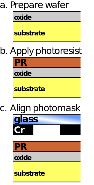
Once this is done, the wafer is prepared for photolithography. An oxide layer on top of the silicon wafer is grown, and then the entire wafer is cleaned to remove contaminants. Once this is done, an adhesion promoter is applied to ensure that the photoresist will stick properly to the wafer. The photoresist is then applied by dispensing a solution of photoresist on to the wafer. The wafer is then spun at extremely high speeds for around half a minute to a minute. Once this is done, the wafer is then baked on a hot plate to get rid of the remaining solvent. In preparation for the exposure, a reticle/photomask for one layer of the process is loaded, and aligned with the wafer. In order to increase resolution, an exposure slit is used to optimize for a smaller exposure area on the reticle/projection lens system, and aberration is reduced.
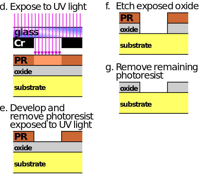
Once all of this preparation is done, the exposure process begins. Intense UV light (currently 193nm) is used to change the exposed photoresist to allow the developer to strip away the exposed area. As a quick aside, the fact that UV light is used to develop the regions to etch away means that only long wavelength light can be used in clean rooms, which gives the clean room a characteristic yellow lighting. Once this is done, the wafer is baked again. This process is done again in order to properly develop the photoresist.
Once the wafer is ready, developer is added. This strips away the photoresist from the exposed regions. The exposed oxide is then etched away. While this process can be done with a liquid agent, modern dry-etch processes ionize a gas in vacuum using an RF cavity that is then shot at the exposed oxide to avoid etching past the exposed portion of the oxide. Once this etching process is complete, the photoresist is removed either through plasma ashing or by washing it off with a resist stripper.
To summarize everything I just said, the process is effectively cleaning the wafer, applying photoresist, exposing the photoresist, developing the photoresist, etching the exposed oxide, then removing the remaining photoresist.
CMOS Fabrication Process / Cmglee / CC BY SA
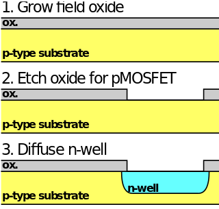
A modern wafer will undergo this process around 50 times or so before creating the final finished chip. You might want to know how all of this etching actually creates transistors, so we’ll once again go over the simplest case, the CMOS inverter. The first lithography pass is used to mark out the area so that we can deposit a well of n-doped silicon that the PMOS will use. Then, the oxide is grown again and a layer of polysilicon is deposited.
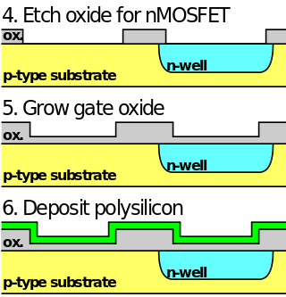
Another lithography pass is done to etch away parts of the oxide, then most of the polysilicon. This leaves a small piece in the center of the exposed substrate composed of silicon dioxide, then polysilicon. If this sounds familiar, it’s because this is the structure of the gate. Once this is done, ion implantation is used to create the sources and drains. The best description I can give of ion implantation is taking an ion and accelerating it to high speeds to embed itself into the targeted area, which dopes the substrate. Once this is done, a layer of nitride is added to prevent further oxide growth, which is then etched again.

Manufacturing: Back End of Line and Back End of Chip

Yet we’re still not done with how the chip is made. We just finished going over what happens in front-end-of-line (FEOL) processing. Now it’s time to go over what happens at back-end-of-line (BEOL) processing. Once the nitride layer is finished, a layer of metal is deposited over the entire system. This layer is then etched again to finish the transistor fabrication process. The result is that all the correct components for source, drain, gate, and body are implanted with metal connectors for input and output for our hypothetical CMOS inverter.
In a real chip, as many as 12 layers are added in this process, which means repeating the metal deposition step 12 times. This step is where all of the transistors are wired together, along with interlayer connections (vias), capacitors (in DRAM), dielectric isolation, and chip to package connectors. Once BEOL processing is complete, the chip is packaged and ready to be used.
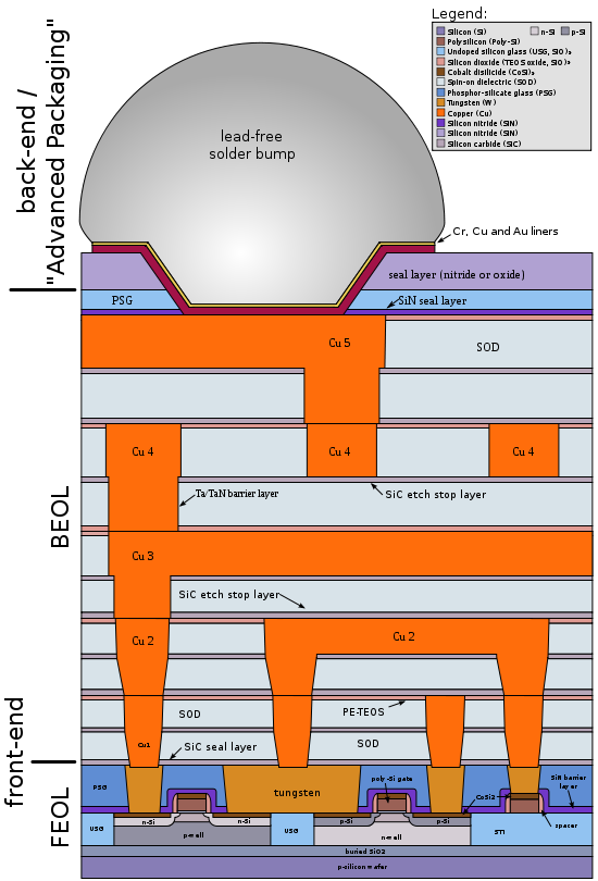
CMOS Chip Structure / Cepheiden / CC BY SA
Of course, this entire production process isn’t perfect. Along the way, the wafer is tested multiple times to ensure that there are no defects from a previous step. If there are too many defects on a wafer, the entire wafer must be thrown away to avoid wasting time and money on further processing. After the FEOL processing is complete, the chip is tested and binned using a wafer prober. After the entire chip is packaged, the chip is tested again to ensure that the entire package is fully functional. The packaging and final testing stages are also known as the back end of chip fabrication.
Recap
To review everything we’ve just gone over, we started with the physics of semiconductors. Then we moved on to the physics of transistors. After that, we went over how to make logic with these transistors. Finally, we went over how to actually make transistors with logic. This would be a good place to stop, but complacency is a terrible reason to do so.
The question now is how to make things faster with less power. To do this, we have to figure out how to make the feature size smaller, in order to pack more transistors closer together. To put things in perspective, 43 years ago in 1971 with the Intel 4004 we had a feature size of 10,000 nanometers. That’s around 455 times as large as the 22nm feature size of what we see in Intel’s Haswell CPUs. Now it’s time to find out how this was achieved.


77 Comments
View All Comments
DanNeely - Friday, October 10, 2014 - link
A lot of them can only make n-type or p-type transistors. While that's not a problem for power or RF transistors; to control energy consumption and heat production you need both types to do CMOS logic gates.JoshHo - Friday, October 10, 2014 - link
While GaAs is popular in MMIC applications, it normally isn't possible to implement CMOS logic with such transistors.Lux88 - Friday, October 10, 2014 - link
Thank you very much for the much needed and very well written and illustrated introduction!How long does it take in real life to make a wafer with chips (with or without the testing)? Does it take hours, days or weeks to get a finished wafer with chips from silicon crystal?
At the end you mention a rate of "100+ wafers per hour", but I understand it as "number of wafers we are working on in parallel" rather than "number of wafers from start to finish".
aicjofs - Friday, October 10, 2014 - link
Time depends on the device and fab. Weeks though. I'd guess the average for any given chip(fron latest greatest down to simple microcontrollers) 3-6 weeks in the fab, another couple for testing packaging.He was talking about replacing a single photo tool(scanner/stepper) that does 100 wafers per hour with ebeam. There can be 10-100 scanners in fab, and as you say working in parallel.
ABR - Friday, October 10, 2014 - link
Great article. Our society has poured vast resources into this area at multiple levels and achieved incredible results. I can't help but think that if we had been motivated to put this kind of engineering effort towards space projects we would not only be colonizing Mars by now, but mining asteroids and running orbital solar panels. Maybe we'll eventually come back to these things, with new powers bestowed by this "inner space" technology. Or maybe not.pepone1234 - Friday, October 10, 2014 - link
This article is amazing!! Thank you for writing this :DKhenglish - Friday, October 10, 2014 - link
You missed the biggest reason why SOI has gone out of fashion from microprocessors. Costs and fabrication are not a big deal. All you do is implant O2 deep into the wafer, then heat it to turn the implanted O2 into SiO2. This is 2 extra steps of 400 or so done when processing a wafer. No big deal.The problem is that there is no more transistor body connection to ground. This means that the body can build up charge like in flash memory. What it ends up doing is skewing the threshold voltage. When doing high voltage work with radio or power electronics with big transistors this is no big deal, but with microprocessors it is a significant. Even worse is this charge depends on the previous state of the transistor and how long it has been in that state, which is difficult to predict, and thus we have unpredictable performance swings with SOI.
JoshHo - Friday, October 10, 2014 - link
This is a PD-SOI issue that falls under history effects mentioned in the article. FD-SOI doesn't have history effects as the body doesn't inherently have mobile charge carriers, which must be generated by band-bending.Khenglish - Friday, October 10, 2014 - link
So if FD-SOI gets rid of body effects then why is SOI not common? I supposed you can't just implant O2 and anneal for FD-SOI? Is sanding the wafer and growing SiO2 what needs to be done?The article also mentions temperatures, but the heatsink is attached to the interconnect side of the CPU instead of the bulk side from my understanding so this should have no impact.
JoshHo - Saturday, October 11, 2014 - link
The biggest issue continues to be cost. While continuing to push bulk CMOS is more expensive in up-front cost, SOI has much higher fluid costs. There's also only one supplier of SOI wafers to my knowledge. (Soitec)