An Introduction to Semiconductor Physics, Technology, and Industry
by Joshua Ho on October 9, 2014 3:00 PM EST- Posted in
- Semiconductors
- CMOS
- Physics
- Industry
- Technology
I must confess that until recently, I wasn’t well-versed in semiconductor physics or technology. While it’s rather easy to understand what a transistor does and some of the terminology thrown around, going deeper was tough. A great deal of the information on the internet is simply too cryptic to understand, even for those that want to learn. Seeing as how this site is all about the results of semiconductor physics and technology, this was the best place to share the knowledge that I've acquired.
Bandgap In Semiconductor / Pieter Kuiper
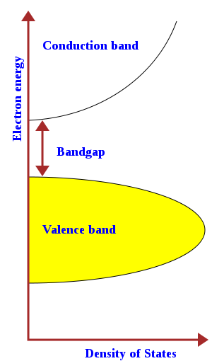
The simplest place to start is the materials. Silicon is incredibly important as a material in the industry because it’s a semiconductor. Of course, the name is self-explanatory, but there’s more to it. The key here is the band structure. Band structure refers to the “bands” of energy levels that form due to the sheer number of orbital states that can be occupied in molecules. Those that understand how electron orbitals work will point out that each energy level is discrete, but due to the sheer number of orbital configurations, a seemingly continuous distribution of energy can be seen. However, relatively large gaps still exist; known as a band gap, these are an energy state that an electron cannot occupy.

Band Filtering Diagram / Nanite
The question now is why this matters. The reason why it does matter is because of the Fermi level, or EF in the photo above. The Fermi level refers to the total chemical potential energy for a system of electrons at absolute zero. If the band lies above the Fermi level, electrons in the band can be delocalized from the atom, which means that it can carry current. This band is called a conduction band. If the band is below the Fermi level, this means that the electron is bound to an atom. This band would be a valence band.
Intrinsically, a semiconductor should have its Fermi level at the midpoint of the band gap. This is true of both insulators and intrinsic semiconductors, but a semiconductor’s band gap is extremely small. In fact, it’s small enough that electrons can jump the band gap as seen in the photo above because of thermal energy that will always exist in real world situations. While this property alone isn't particularly useful for digital logic, doping a semiconductor can have significant effects on the band structure. This means that the distribution of electrons in the valence band or conduction band will change.
This is where I have to introduce even more terminology. Depending on how the distribution is changed, a semiconductor is dubbed either a p-type or n-type semiconductor. If the band structure is such that free electrons are more easily generated, it becomes an n-type semiconductor. If the structure is such that electron “holes” are generated, it becomes a p-type semiconductor. In this case, electron holes refers to a place where an electron could exist, but doesn’t. Such a hole still conducts current. Look carefully at the p-type diagram once again. Because the valence band is so close to the Fermi level, electrons tend to stay in the valence band at lower orbitals. This is means that there are "holes" where an electron could be, which makes it a charge carrier. It's also worth noting that the diagram above isn't totally accurate, as doping normally introduces more bands instead of shifting their positions, but the concept is the same.
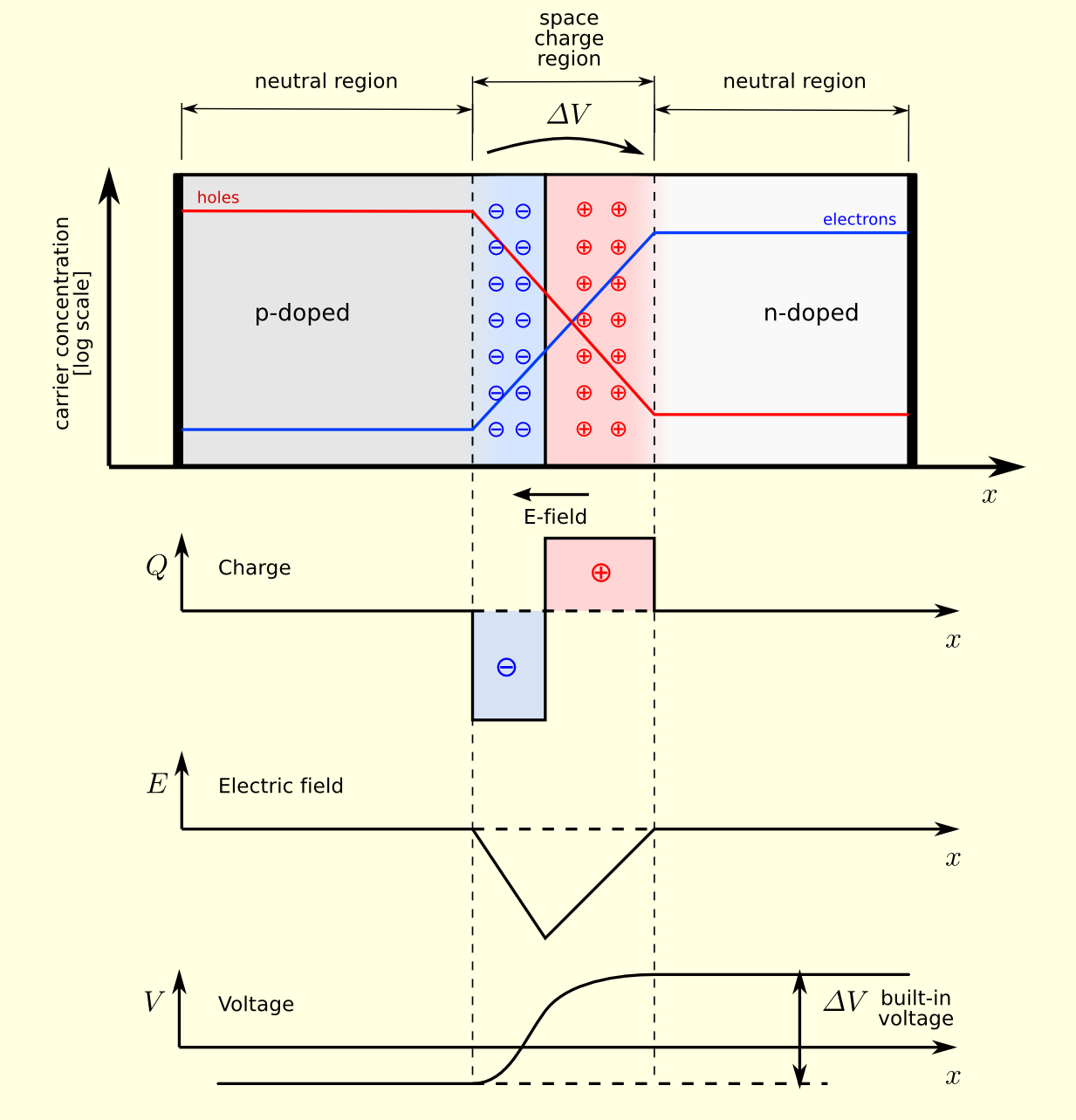
PN Junction Equilibrium / TheNoise / CC BY SA
What really makes things interesting is when a p-type and n-type semiconductor are placed next to each other. Because p-type semiconductors tend to have electron holes and n-type semiconductors tend to have an excess of electrons, there will be a diffusion of holes and electrons to try and equalize charge at the junction. Because of this diffusion process, the area around the junction becomes charged positively at the n-doped region and negatively at the p-doped region. This happens because the n-doped region is losing electrons, making the area positive while the p-doped region is losing holes, therefore becoming negative. The result is that an electric field is generated which opposes this diffusion and eventually reaches equilibrium. The area where this process occurs is called the depletion layer, as these ionized areas are stripped of charge carriers and therefore unable to carry current with the band structure that already exists.

PN Band / Saumitra R Mehrotra & Gerhard Klimeck / CC BY
This p-n junction is incredibly important in solid state electronics. In fact, the system we just described can be used as a diode, which is a device that only allows current to flow in a single direction. If a battery is connected with the positive terminal at the p-type semiconductor and the negative on the n-type semiconductor, the holes in the p-type and the electrons in n-type are all pushed towards the junction, which causes the depletion zone to shrink. This means that the electric field repelling the current decreases, and current is allowed to flow across the junction.


77 Comments
View All Comments
DanNeely - Friday, October 10, 2014 - link
A lot of them can only make n-type or p-type transistors. While that's not a problem for power or RF transistors; to control energy consumption and heat production you need both types to do CMOS logic gates.JoshHo - Friday, October 10, 2014 - link
While GaAs is popular in MMIC applications, it normally isn't possible to implement CMOS logic with such transistors.Lux88 - Friday, October 10, 2014 - link
Thank you very much for the much needed and very well written and illustrated introduction!How long does it take in real life to make a wafer with chips (with or without the testing)? Does it take hours, days or weeks to get a finished wafer with chips from silicon crystal?
At the end you mention a rate of "100+ wafers per hour", but I understand it as "number of wafers we are working on in parallel" rather than "number of wafers from start to finish".
aicjofs - Friday, October 10, 2014 - link
Time depends on the device and fab. Weeks though. I'd guess the average for any given chip(fron latest greatest down to simple microcontrollers) 3-6 weeks in the fab, another couple for testing packaging.He was talking about replacing a single photo tool(scanner/stepper) that does 100 wafers per hour with ebeam. There can be 10-100 scanners in fab, and as you say working in parallel.
ABR - Friday, October 10, 2014 - link
Great article. Our society has poured vast resources into this area at multiple levels and achieved incredible results. I can't help but think that if we had been motivated to put this kind of engineering effort towards space projects we would not only be colonizing Mars by now, but mining asteroids and running orbital solar panels. Maybe we'll eventually come back to these things, with new powers bestowed by this "inner space" technology. Or maybe not.pepone1234 - Friday, October 10, 2014 - link
This article is amazing!! Thank you for writing this :DKhenglish - Friday, October 10, 2014 - link
You missed the biggest reason why SOI has gone out of fashion from microprocessors. Costs and fabrication are not a big deal. All you do is implant O2 deep into the wafer, then heat it to turn the implanted O2 into SiO2. This is 2 extra steps of 400 or so done when processing a wafer. No big deal.The problem is that there is no more transistor body connection to ground. This means that the body can build up charge like in flash memory. What it ends up doing is skewing the threshold voltage. When doing high voltage work with radio or power electronics with big transistors this is no big deal, but with microprocessors it is a significant. Even worse is this charge depends on the previous state of the transistor and how long it has been in that state, which is difficult to predict, and thus we have unpredictable performance swings with SOI.
JoshHo - Friday, October 10, 2014 - link
This is a PD-SOI issue that falls under history effects mentioned in the article. FD-SOI doesn't have history effects as the body doesn't inherently have mobile charge carriers, which must be generated by band-bending.Khenglish - Friday, October 10, 2014 - link
So if FD-SOI gets rid of body effects then why is SOI not common? I supposed you can't just implant O2 and anneal for FD-SOI? Is sanding the wafer and growing SiO2 what needs to be done?The article also mentions temperatures, but the heatsink is attached to the interconnect side of the CPU instead of the bulk side from my understanding so this should have no impact.
JoshHo - Saturday, October 11, 2014 - link
The biggest issue continues to be cost. While continuing to push bulk CMOS is more expensive in up-front cost, SOI has much higher fluid costs. There's also only one supplier of SOI wafers to my knowledge. (Soitec)