An Introduction to Semiconductor Physics, Technology, and Industry
by Joshua Ho on October 9, 2014 3:00 PM EST- Posted in
- Semiconductors
- CMOS
- Physics
- Industry
- Technology
Manufacturing: Making Wafers
To make a computer chip, it all starts with the Czochralski process. The first step of this process is to take extremely pure silicon and melt it in a crucible that is often made of quartz. Doping material can also be added at this stage, to change the properties of the final crystal. Once this is done, a single seed crystal is dipped into the molten silicon, then carefully pulled up with a specific rotation rate. This produces a piece of monocrystalline silicon that is then sliced into wafers. These wafers can be up to 300mm in diameter at present and around .75mm thick, and they are polished to ensure that the surface is as regular and flat as possible.
Manufacturing: Photolithography/FEOL
Photolithography Etching Process / Cmglee / CC BY SA
Scanning Stepper Middle Exposure / Everyguy
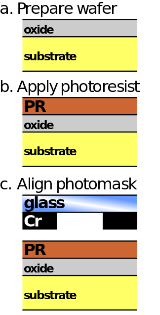
Once this is done, the wafer is prepared for photolithography. An oxide layer on top of the silicon wafer is grown, and then the entire wafer is cleaned to remove contaminants. Once this is done, an adhesion promoter is applied to ensure that the photoresist will stick properly to the wafer. The photoresist is then applied by dispensing a solution of photoresist on to the wafer. The wafer is then spun at extremely high speeds for around half a minute to a minute. Once this is done, the wafer is then baked on a hot plate to get rid of the remaining solvent. In preparation for the exposure, a reticle/photomask for one layer of the process is loaded, and aligned with the wafer. In order to increase resolution, an exposure slit is used to optimize for a smaller exposure area on the reticle/projection lens system, and aberration is reduced.
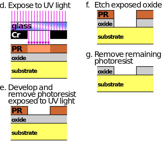
Once all of this preparation is done, the exposure process begins. Intense UV light (currently 193nm) is used to change the exposed photoresist to allow the developer to strip away the exposed area. As a quick aside, the fact that UV light is used to develop the regions to etch away means that only long wavelength light can be used in clean rooms, which gives the clean room a characteristic yellow lighting. Once this is done, the wafer is baked again. This process is done again in order to properly develop the photoresist.
Once the wafer is ready, developer is added. This strips away the photoresist from the exposed regions. The exposed oxide is then etched away. While this process can be done with a liquid agent, modern dry-etch processes ionize a gas in vacuum using an RF cavity that is then shot at the exposed oxide to avoid etching past the exposed portion of the oxide. Once this etching process is complete, the photoresist is removed either through plasma ashing or by washing it off with a resist stripper.
To summarize everything I just said, the process is effectively cleaning the wafer, applying photoresist, exposing the photoresist, developing the photoresist, etching the exposed oxide, then removing the remaining photoresist.
CMOS Fabrication Process / Cmglee / CC BY SA
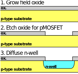
A modern wafer will undergo this process around 50 times or so before creating the final finished chip. You might want to know how all of this etching actually creates transistors, so we’ll once again go over the simplest case, the CMOS inverter. The first lithography pass is used to mark out the area so that we can deposit a well of n-doped silicon that the PMOS will use. Then, the oxide is grown again and a layer of polysilicon is deposited.
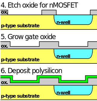
Another lithography pass is done to etch away parts of the oxide, then most of the polysilicon. This leaves a small piece in the center of the exposed substrate composed of silicon dioxide, then polysilicon. If this sounds familiar, it’s because this is the structure of the gate. Once this is done, ion implantation is used to create the sources and drains. The best description I can give of ion implantation is taking an ion and accelerating it to high speeds to embed itself into the targeted area, which dopes the substrate. Once this is done, a layer of nitride is added to prevent further oxide growth, which is then etched again.

Manufacturing: Back End of Line and Back End of Chip

Yet we’re still not done with how the chip is made. We just finished going over what happens in front-end-of-line (FEOL) processing. Now it’s time to go over what happens at back-end-of-line (BEOL) processing. Once the nitride layer is finished, a layer of metal is deposited over the entire system. This layer is then etched again to finish the transistor fabrication process. The result is that all the correct components for source, drain, gate, and body are implanted with metal connectors for input and output for our hypothetical CMOS inverter.
In a real chip, as many as 12 layers are added in this process, which means repeating the metal deposition step 12 times. This step is where all of the transistors are wired together, along with interlayer connections (vias), capacitors (in DRAM), dielectric isolation, and chip to package connectors. Once BEOL processing is complete, the chip is packaged and ready to be used.
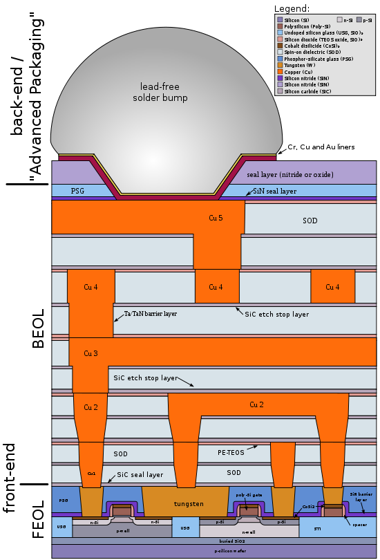
CMOS Chip Structure / Cepheiden / CC BY SA
Of course, this entire production process isn’t perfect. Along the way, the wafer is tested multiple times to ensure that there are no defects from a previous step. If there are too many defects on a wafer, the entire wafer must be thrown away to avoid wasting time and money on further processing. After the FEOL processing is complete, the chip is tested and binned using a wafer prober. After the entire chip is packaged, the chip is tested again to ensure that the entire package is fully functional. The packaging and final testing stages are also known as the back end of chip fabrication.
Recap
To review everything we’ve just gone over, we started with the physics of semiconductors. Then we moved on to the physics of transistors. After that, we went over how to make logic with these transistors. Finally, we went over how to actually make transistors with logic. This would be a good place to stop, but complacency is a terrible reason to do so.
The question now is how to make things faster with less power. To do this, we have to figure out how to make the feature size smaller, in order to pack more transistors closer together. To put things in perspective, 43 years ago in 1971 with the Intel 4004 we had a feature size of 10,000 nanometers. That’s around 455 times as large as the 22nm feature size of what we see in Intel’s Haswell CPUs. Now it’s time to find out how this was achieved.


77 Comments
View All Comments
danjw - Thursday, October 9, 2014 - link
I am wondering if we haven't already hit the limits of current technology. TSMC doesn't seem to be able to produce anything more powerful than a SOC for phones and tablets on their 20nm process. While Intel seems to think they will have 14nm desktop and notebook parts out in the second quarter of next year, I wonder if they really will. Right now all we have seen from them at 14nm is similar to what TSMC is able to do at 20nm.This really concerns me as far as technology stagnating until the next big thing comes along.
Homeles - Thursday, October 9, 2014 - link
There's no end in sight. About a year ago, perhaps a little earlier, the 7 or 5nm nodes were seen as the end of Moore's Law. Advancements have been made since then, though, and scaling past the 5nm node is very likely. 10nm's "recipe" is basically all finished at Intel at this point, with "all" that's left to do at this point being increasing the yields. EUV is making good progress, finally, and should be ready for insertion at Intel's 7nm node (if they skipped it for 10nm, which they likely did).14nm has been in production for quite some time now, with Broadwell first landing in tablets later this month. The chances that Broadwell won't make it to the desktop and notebook market around the middle of next year are essentially zero.
We're still also on schedule to have 450mm wafers introduced by the end of the decade, which would reduce costs by ~30%.
Even not looking at Intel, TSMC has millions of 20nm-based products on the market right now. 20nm is roughly twice as dense as its 28nm predecessor. It doesn't really make sense to be so skeptical of progress, given that the proof pudding has already been delivered.
danjw - Thursday, October 9, 2014 - link
All those 20nm products are not desktop or notebook CPUs or GPUs, which they lead AMD and Nvidia to believe they would be able to do. Intel is way behind its original estimates to get Broadwell out, and that just in table SOCs. Intel wanted badly to get Broadwell parts out for the new school year, then it was Christmas, now it is Q2 of 2015. Yes, I think there is plenty of reason to be skeptical.EMM81 - Monday, October 13, 2014 - link
Your facts are all incorrect...If you can produce an SOC you already have all of the capability to produce GPU's or CPU's since it has logic, SRAM and graphics components already. Broadwell parts are already in the hands of vendors NOW and are being sold this year and they are not SOC's they are low power full core chips. 14nm Broadwell chips are in no way equivalent to 20nm TSMC chips. A fab can use the additional capability of a new node in different ways. They can reduce density to make chips cheaper to make, increase performance, decrease power and all of these things will be done in different ratios depending on the product. You need to work on detailed reasoning and apples to apples comparisons.errorr - Thursday, October 9, 2014 - link
The problem is that the only real advancements are more expensive per transistor and I doubt they will change.The great thing about process shrinks is that it reduces the cost per transistor.
Also I doubt EUV will ever work. It has been almost ready and a couple years away for a decade. Tell me when you don't need MW levels of power to get usable light to a wafer and maybe I will consider it.
450mm wafers have also been just a couple years away for at least 15 years. I'll believe the 2020 hype when I actually see it.
The way to the next node is easy and everyone knows they can use triple patterning. Nobody wants that because of the expense is huge already and every single circuit would have to be redrawn due to limitations on the pokygons.
I don't know what's next but the only people expecting EUV to pan out are the people who have spent billions trying to make it work and failing.
ShieTar - Friday, October 10, 2014 - link
EUV is not "almost ready", it has been commercially available for 2 years now.http://www.zeiss.com/semiconductor-manufacturing-t...
Khenglish - Thursday, October 9, 2014 - link
The problem with smaller processes is not physically producing them. The problem is that they start getting slower than larger processes. This is due to 2 reasons.1. Narrower, more resistive interconnects.
2. Increase in channel doping levels due to not having enough dopant atoms to form a P-N junction as processes increase.
1. As process sizes shrink, so do interconnects. Resistance is dependent on cross sectional area and length of the wire. As you shrink a process, the cross sectional area drops at a squared rate, while length drops at a linear rate. The end result is that wires become linearly more resistive as the process shrinks. Keeping wire length down due to resistance is also a big reason why individual core transistor counts have not been going up significantly. The cores need to stay small to keep the wire length down. Repeaters to boost current drive ability on long wires has been around starting at around 90nm.
2. If you want a 10nm process, you probably have a gate length of 10nm. The volume of a 10nm cube is 10^-18 cm^-3. High doping levels are those above around 10^17 atoms per cm. If we take a high doping level of say 10^18 atoms per cm, then we have only one single dopant atom in the entire channel region of the transistor. This means that if you are one atom off, you lose a transistor, which is difficult not to do with over 1B transistors in a microprocessor. You can dope up to around 10^21 cm^-3, but then your electron and hole mobility are terrible. Mobility is directly proportional to how much current a transistor can push, so as mobility drops performance drops. See this link for what happens to mobility as dopant levels increase.
http://ecee.colorado.edu/~bart/book/mobility.gif
abufrejoval - Saturday, October 11, 2014 - link
From what I read the problem isn't as much phyiscal or technical feasability as economical viability: Moore's law was mostly about the ability to deliver more power at a lower price for the end consumer pushing the technology. Now the economical yields of process shrinks are diminishing to the point where further shrinks won't pay for themselves.DanNeely - Thursday, October 9, 2014 - link
If you're also interested in how simpler transistors are made; hack-a-day's hosted a video lecture from someone who was producing chips with a handful of transistors on them in her home lab a few years ago.http://hackaday.com/2010/03/10/jeri-makes-integrat...
anexanhume - Thursday, October 9, 2014 - link
Graphene isn't dead in the water. There are ways to create a bandgap, for example using bilayer graphene and introducing a gap via electric fields or doping.http://www-als.lbl.gov/index.php/contact/56-bilaye...
Then you can take advantage of its remarkable carrier mobility. Mass production remains a huge issue, and I also have concerns about its effect on living creatures and the environment. http://www.gizmag.com/graphene-bad-for-environment...