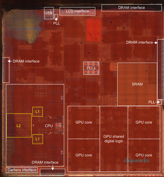
An Introduction to Semiconductor Physics, Technology, and Industry
by Joshua Ho on October 9, 2014 3:00 PM EST- Posted in
- Semiconductors
- CMOS
- Physics
- Industry
- Technology
I must confess that until recently, I wasn’t well-versed in semiconductor physics or technology. While it’s rather easy to understand what a transistor does and some of the terminology thrown around, going deeper was tough. A great deal of the information on the internet is simply too cryptic to understand, even for those that want to learn. Seeing as how this site is all about the results of semiconductor physics and technology, this was the best place to share the knowledge that I've acquired.
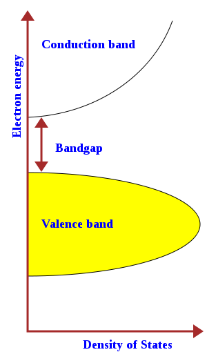
Bandgap In Semiconductor / Pieter Kuiper
The simplest place to start is the materials. Silicon is incredibly important as a material in the industry because it’s a semiconductor. Of course, the name is self-explanatory, but there’s more to it. The key here is the band structure. Band structure refers to the “bands” of energy levels that form due to the sheer number of orbital states that can be occupied in molecules. Those that understand how electron orbitals work will point out that each energy level is discrete, but due to the sheer number of orbital configurations, a seemingly continuous distribution of energy can be seen. However, relatively large gaps still exist; known as a band gap, these are an energy state that an electron cannot occupy.

Band Filtering Diagram / Nanite
The question now is why this matters. The reason why it does matter is because of the Fermi level, or EF in the photo above. The Fermi level refers to the total chemical potential energy for a system of electrons at absolute zero. If the band lies above the Fermi level, electrons in the band can be delocalized from the atom, which means that it can carry current. This band is called a conduction band. If the band is below the Fermi level, this means that the electron is bound to an atom. This band would be a valence band.
Intrinsically, a semiconductor should have its Fermi level at the midpoint of the band gap. This is true of both insulators and intrinsic semiconductors, but a semiconductor’s band gap is extremely small. In fact, it’s small enough that electrons can jump the band gap as seen in the photo above because of thermal energy that will always exist in real world situations. While this property alone isn't particularly useful for digital logic, doping a semiconductor can have significant effects on the band structure. This means that the distribution of electrons in the valence band or conduction band will change.
This is where I have to introduce even more terminology. Depending on how the distribution is changed, a semiconductor is dubbed either a p-type or n-type semiconductor. If the band structure is such that free electrons are more easily generated, it becomes an n-type semiconductor. If the structure is such that electron “holes” are generated, it becomes a p-type semiconductor. In this case, electron holes refers to a place where an electron could exist, but doesn’t. Such a hole still conducts current. Look carefully at the p-type diagram once again. Because the valence band is so close to the Fermi level, electrons tend to stay in the valence band at lower orbitals. This is means that there are "holes" where an electron could be, which makes it a charge carrier. It's also worth noting that the diagram above isn't totally accurate, as doping normally introduces more bands instead of shifting their positions, but the concept is the same.
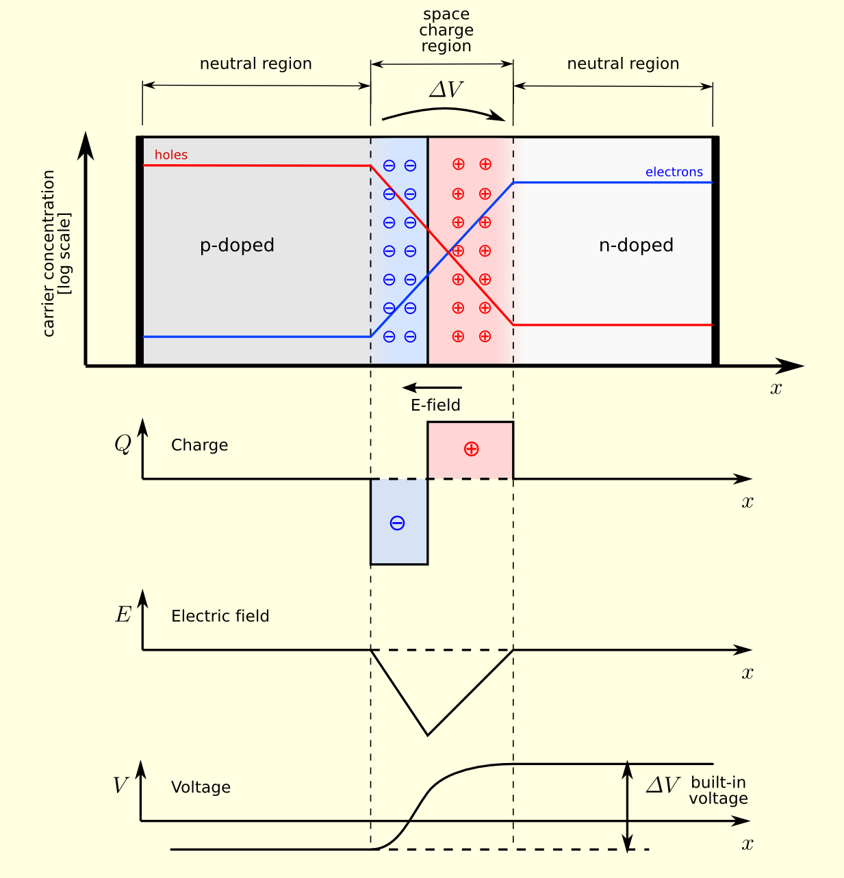
PN Junction Equilibrium / TheNoise / CC BY SA
What really makes things interesting is when a p-type and n-type semiconductor are placed next to each other. Because p-type semiconductors tend to have electron holes and n-type semiconductors tend to have an excess of electrons, there will be a diffusion of holes and electrons to try and equalize charge at the junction. Because of this diffusion process, the area around the junction becomes charged positively at the n-doped region and negatively at the p-doped region. This happens because the n-doped region is losing electrons, making the area positive while the p-doped region is losing holes, therefore becoming negative. The result is that an electric field is generated which opposes this diffusion and eventually reaches equilibrium. The area where this process occurs is called the depletion layer, as these ionized areas are stripped of charge carriers and therefore unable to carry current with the band structure that already exists.

PN Band / Saumitra R Mehrotra & Gerhard Klimeck / CC BY
This p-n junction is incredibly important in solid state electronics. In fact, the system we just described can be used as a diode, which is a device that only allows current to flow in a single direction. If a battery is connected with the positive terminal at the p-type semiconductor and the negative on the n-type semiconductor, the holes in the p-type and the electrons in n-type are all pushed towards the junction, which causes the depletion zone to shrink. This means that the electric field repelling the current decreases, and current is allowed to flow across the junction.


77 Comments
View All Comments
Khenglish - Thursday, October 9, 2014 - link
Curving the wafer actually has major impacts on electronic operation. For example wafer bending is currently done by implanting Germanium into the wafer for PFETs. Because Ge is larger than Si, this causes the wafer to bend. This bend increases hole mobility making PFETs more conductive and faster, but slows down NFETs, thus manufacturers implant Ge only at PFET locations. This processes of bending the wafer by implanting Ge is strained silicon, and 1st started showing up around the 130nm era. It is done because for similarly sized transistors, NFETs are around 2.7x more conductive than PFETs without strained silicon.EMM81 - Monday, October 13, 2014 - link
There is definitely no curving or any wafer. Ge is used to strain the silicon crystal latice. Ge is in the same group on the periodic table and forms the same diamond cubic crystal structure. Grading a fraction of Ge (larger atoms longer bond lengths) into the Silicon latice the silicon bonds effectively get stretched (see image in article). This has a physical effect on the mobility of electrons and holes. Curving a wafer is a non-starter as NONE of the standard processing techniques would work...wafers have to be not only flat but ultra flat for litho optics, dry etch, wet etch spinners, ion implanters...hlovatt - Thursday, October 9, 2014 - link
Great article. More please!witeken - Thursday, October 9, 2014 - link
Awesome, thanks for the great article.However, 22nm doesn't have a single feature size of 22nm. It's just a name, and so are 28nm, 20nm, 16nm, 14nm,...
For example, the fins of 22nm are 8nm while the gate pitch is 90nm. (http://images.anandtech.com/doci/8367/14nmFeatureS...
Khenglish - Thursday, October 9, 2014 - link
When you hear 22nm, 32nm, 16nm, etc the number you are hearing is the smallest feature size that can be imprinted via lithography. This is not necessarily the smallest feature size than can be implemented on the process.EMM81 - Monday, October 13, 2014 - link
This is not true. Node size was loosely defined as the half pitch of either the poly-silicon gate or the tightest metal pitch. The node size designation however, has not followed the minimum half pitch for many technologies, from any of the fabs. Node size is now a purely marketing term. If a fab were to implement HKMG, strained silicon...these things would not necessarily have any effect on the dimensions of transistors but they would result in improvements to the chip performance. Density is only 1 component that plays into node designation these days and even then density of the transistors is being tightened by some fabs while leaving the density of the upper layers unchanged.Khenglish - Wednesday, October 15, 2014 - link
Again just because lithographic features can be made a certain size does not mean you make everything that size. Maybe there is just one minor feature that is really that size. I'm saying that process size is the minimum size that can cut by the ebeam into a lithography mask and transferred if the design calls for it. This is why when looking at a processor that the feature size is so hard to quantify. Just one feature at whatever they advertise can let them call it that number. Yes feature size doesn't need to have anything to do with density or performance and is mostly a marketing thing.Keisari - Thursday, October 9, 2014 - link
A very necessary article. Great initiative!martixy - Thursday, October 9, 2014 - link
There's probably something to be said about breezing through this(of my own free will moreover), while having such a hard time with the exact same material from the textbook.Go figure.
Murloc - Thursday, October 9, 2014 - link
It's meant to be intuitive and summarized in a limited amount of space. That's why it's easy to read. It has way less depth than a textbook.