AMD Beema/Mullins Architecture & Performance Preview
by Anand Lal Shimpi on April 29, 2014 12:00 AM EST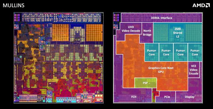
When AMD launched its Kabini and Temash APUs last year it delivered a compelling cost/performance story, but its power story wasn’t all that impressive. Despite being built out of relatively low power components, nearly all of AMD’s entry level APUs carried 15W TDPs, with a couple weighing in at 8 - 9W and only a single 1GHz dual-core part dropping down to 3.9W. By comparison, Intel was shipping full blown Haswell Ultrabook parts at 15W - offering substantially better CPU performance, in a similar thermal envelope (although at a higher cost). The real disruption for AMD was Intel’s Bay Trail, which showed up with a similar looking micro architecture running at substantially higher clock speeds and TDPs below 8W.
AMD seemed to have all of the right pieces to build a power efficient mobile SoC, but for some reason we weren’t seeing it. Today that begins to change with the the successors to Kabini and Temash.
Codenamed Beema and Mullins, these are the 2014 updates to Kabini and Temash (respectively). Beema is aimed at entry level notebooks, while Mullins targets tablets. For now, both are designed for Windows machines. Although I suspect we’ll eventually see AMD address the native Android market head on, for now AMD is relying on running Android on top of Windows for those who really want it. No word on if/when we’ll get a socketed Beema for entry level desktops.
Like their predecessors, Beema and Mullins combine four low power AMD x86 cores (Puma+ this time, instead of Jaguar) with 128 GCN based Radeon GPU cores. AMD will continue to offer a couple of dual-core SKUs, but they are harvested from a quad-core die. AMD remains unwilling to release official die area figures, but there is a slight increase in transistor count:
| AMD/Intel Transistor Count & Die Area Comparison | |||||
| SoC | Process Node | Transistor Count | Die Area | ||
| AMD Zacate | TSMC 40nm | 450M+ | 75mm2 | ||
| AMD Kabini/Temash | TSMC 28nm | 914M | ~107mm2 (est) | ||
| AMD Beema/Mullins | GF 28nm | 930M | ~107mm2 (est) | ||
| AMD Llano | GF 32nm SOI | 1.18B | 228mm2 | ||
| AMD Trinity/Richland | GF 32nm SOI | 1.30B | 246mm2 | ||
| AMD Kaveri | GF 28nm SHP | 2.41B | 245mm2 | ||
| Intel Haswell (4C/GT2) | Intel 22nm | 1.40B | 177mm2 | ||
I’d expect a similar die size to Kabini/Temash. It’s interesting to note that these SoCs have a transistor count somewhere south of Apple’s A7.
Puma+ is based on the same micro architecture as Jaguar. We’re still looking at a 2-wide OoO design with the same number of execution units and data structures inside the chip. The memory interface remains unchanged as well at 64-bits wide. These new SoCs are still built on the same 28nm process as their predecessor. The process however has seen some improvements. Not only are both the CPU and GPU designs slightly better optimized for lower power operation, but both benefit from improvements to the manufacturing process resulting in substantial decreases in leakage current.
AMD claims a 19% reduction in core leakage/static current for Puma+ compared to Jaguar at 1.2V, and a 38% reduction for the GPU. The drop in leakage directly contributes to a substantially lower power profile for Beema and Mullins.
AMD also went in and tweaked the SoC’s memory interface. Kabini/Temash had a standard PC-like DDR3 memory interface. All of the complexity required for broad memory module compatibility and variations in trace routing was handed by the controller itself. This not only added complexity to the DDR3 interface but power as well. With Beema and Mullins, AMD took a page from the smartphone SoC design guide and traded flexibility for power. These platforms now ship with more strict guidelines as to what sort of memory can be used on board and how traces must be routed. The result is a memory interface that shaves off more than 500mW when in this more strict, low power mode. OEMs looking to ship a design with socketed DRAM can still run the memory interface in a higher power mode to ensure memory compatibility.
These SoCs won’t be available in a PoP configuration unfortunately - OEMs will have to rely on discrete DRAM packages rather than a fully integrated solution. Beema/Mullins also show up to a 200mW reduction in power consumed by the display interface compared to Kabini/Temash.
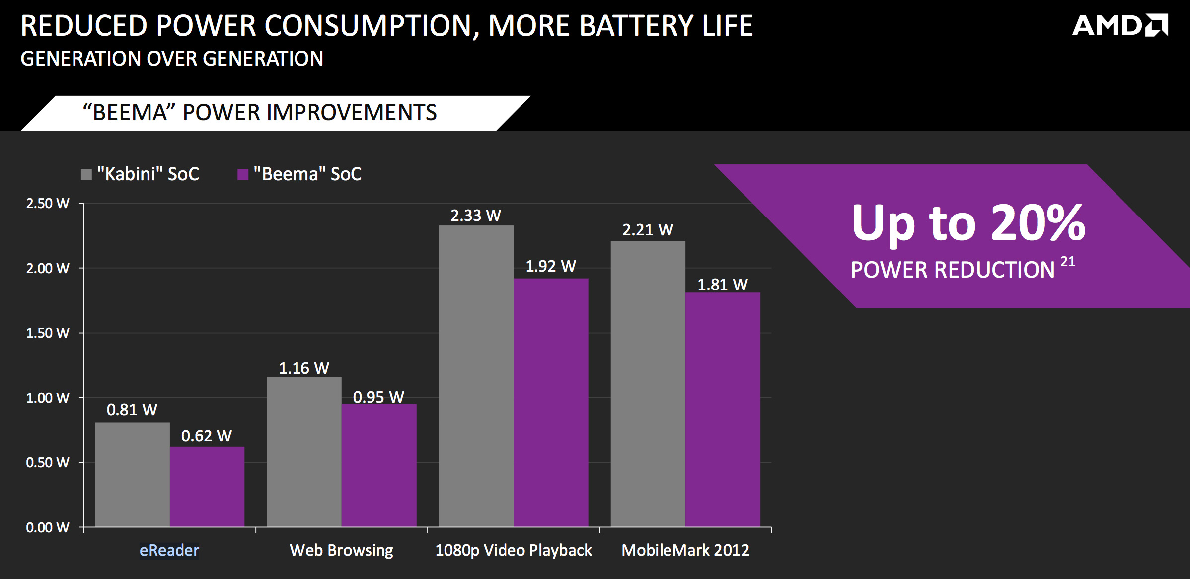
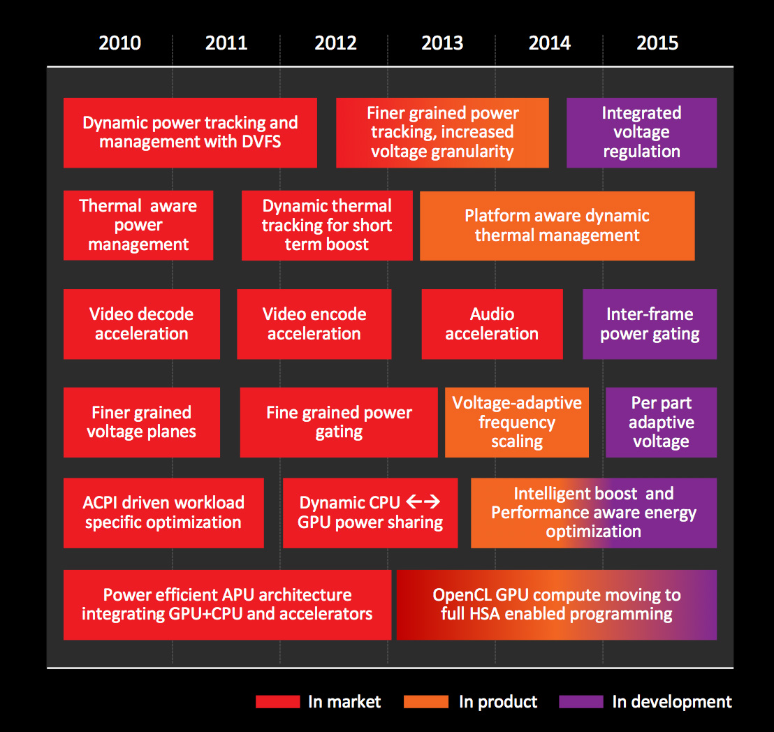
The combination of all of this is 20% lower idle power compared to the previous generation of AMD entry level and low power APUs. AMD put together a nice graph illustrating its progress over the years:
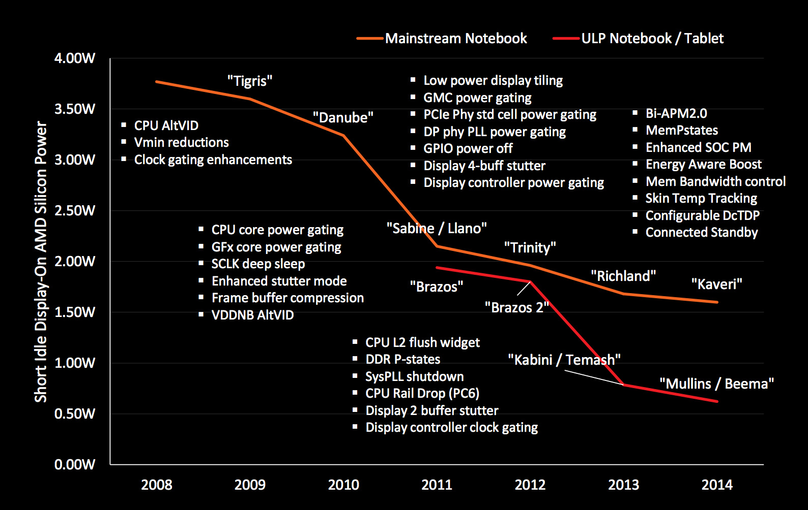
Beema and Mullins are definitely in a good place, however they still do consume more power at idle than the smartphone SoCs we typically find in iOS and Android tablets. AMD isolated APU power for the graph above and is using an “eReader” workload (aka display on but not animating, system otherwise idle). It just so happens I gathered similar data for our 2013 Nexus 7 review. The workloads and measurements are different (AMD isolates APU power, I’m looking at total platform power minus display) but it’s enough to put things in perspective:
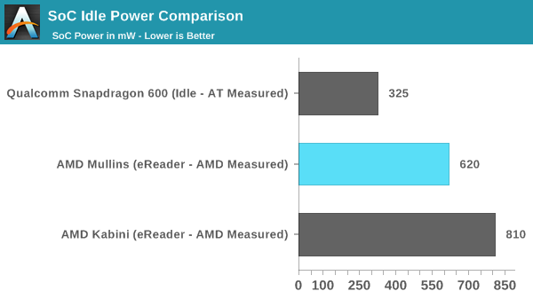
AMD has dropped power consumption considerably over the years, but it’s still not as power efficient as high end mobile silicon.
AMD sees no value in supporting Microsoft's Connected Standby standard at this point, which makes sense given the limited success of Windows 8 tablets. Once again this seems to point to AMD eventually adopting Android for its tablet aspirations.
Looking forward, AMD has more tricks up its sleeve to continue to drive power down. Most interesting on the list? We’ll see an integrated voltage regulator (ala Haswell’s FIVR) from AMD in 2015.


82 Comments
View All Comments
duploxxx - Tuesday, April 29, 2014 - link
Rival really here is intel, nowhere compared in this reviewssj3gohan - Tuesday, April 29, 2014 - link
You do realize that this is an AMD advertisement, not an actual journalistic article? Look at the top of the page: it says AMD Center.DanNeely - Tuesday, April 29, 2014 - link
Anything tagged AMD gets the AMD Center branding, regardless of the content (which's lead to an occasional giggle-snort situation in with articles that are 99% Intel/nVidia but mention AMD for comparison purposes). Look at the by line, this was written by Anand, not one of the AMD PR drones.mfoley93 - Wednesday, April 30, 2014 - link
There is also an Intel Center and nVIDIA Center that all articles about their respective products go in, does that make all articles about them advertisements as well?ruggia - Tuesday, April 29, 2014 - link
If you want a rough comparison with BayTrail, go check out the benchmarks at Toms' (or pull up Anand's old Kaveri articles). You'll be amazed.ruggia - Tuesday, April 29, 2014 - link
*Kabiniduploxxx - Friday, May 2, 2014 - link
there is info here and you see that it can very well compete with intel parts or even better in many parts. the problem is that many bench just wont run on the low end atom GPU wise :). you need the celeron version to compare performance to mullinAnand Lal Shimpi - Tuesday, April 29, 2014 - link
All of the CPU tests are compared to Intel parts, including the direct competitor: Intel's Bay Trail based Atom both in the ASUS Transformer Book T100 as well as numbers from Intel's Bay Trail tech day using the Atom Z3770.Stuka87 - Tuesday, April 29, 2014 - link
Intel chips are in several of the graphs, and is talked about specifically in several places.Did you even read the article?
MrSpadge - Tuesday, April 29, 2014 - link
A substantial performance increase over its predecessor is regressive? And if you insist comparing to AMDs big cores.. well, have fun putting these into a tablet!2x the power consumption? You seem to refer to idle power compared to Snapdragon 600, a SoC which is significantly slower and hence - just like the big cores - in a different category.
Beema / Mullins seems to occupy a very interesting point on the performance/power/price curves. It's obviously not for smartpones yet and neither for big gaming rigs. But for anything in between it's at least an intersting option.