Plextor M6S & M6M (256GB) Review
by Kristian Vättö on April 10, 2014 6:00 AM ESTThe Math of Marketing: Not All 19nm NAND Is the Same
Almost a year ago, Toshiba/SanDisk announced their second generation 19nm NAND. It's typical for NAND manufacturers to use the same process node for more than one generation because manufacturers can cut the die size by increasing either the page, block, or die capacity (or even all three at once), which will lead to lower production costs. However, Toshiba/SanDisk had already upped the page size to 16KB and the die capacity remained at 64Gbit, so how did they manage to decrease the die size by 17%? We'll need to dig a little deeper into the die to find that out but first (no, I'm not gonna take a selfie) let's quickly revise how NAND works.
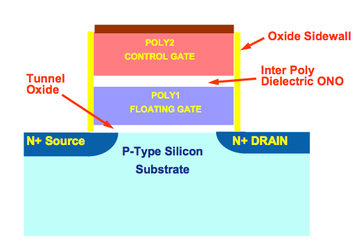
That is what a cross-section of a NAND cell looks like when it's turned into nice colorful graph. This is what it looks like in practice:
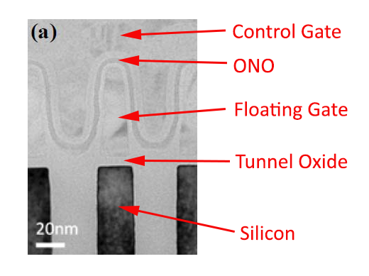
Not as nice as the graph above, right? The reason we need the cross-section photo is because the graph is a bit too simplified and doesn't show one crucial thing: the control gate isn't something that just sits on top of the floating gate and the inter poly dielectric - it actually wraps around the whole floating gate. That's to keep the capacitance between the control and floating gates as high as possible, which in turn helps to maintain the charge in the floating gate and increase performance (the math behind this is actually more simple than you would expect but I'm not going to scare people off with a bunch of equations here). B ut that is just one cell. To truly understand the structure of NAND, we need to zoom out a bit.
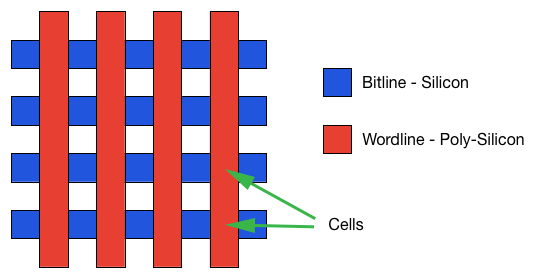
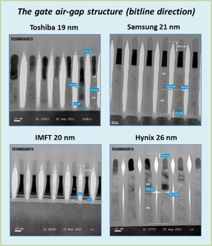
That is what a bunch of NAND cells look like from above. The bitlines (i.e. silicon in the cross-section photo above) are made of silicon and on top of them are the wordlines that are also known as control gates. At every intersection of a bitline and wordline, there is one cell capable of holding one (SLC), two (MLC) or three (TLC) bits of data.
Traditionally cells are symmetrical. The process node refers to the size of one cell, so in the case of 20nm NAND, the cell size would be 20nm x 20nm. However, there is no rule against making an asymmetrical cell and that is in fact what Toshiba/SanDisk did with their first generation 19nm NAND. Instead of being a symmetrical 19nm x 19nm design, the cell size was 19nm x 26nm. Compared to IMFT's symmetrical 20nm design, the actual cell size is quite a bit larger (494 nm2 vs 400 nm2 ), yet in terms of marketing Toshiba's/SanDisk's "19nm" NAND was smaller and more advanced.
You could call that cheating but there is a good technical reason as to why building an asymmetrical design makes sense. As I mentioned earlier, the wordline (control gate) wraps around every floating gate and between them is an insulating inter poly dielectric (often referred to as ONO due to its oxide-nitride-oxide structure, or just IPD). Since the floating gate is where the electrons are stored, it needs to be insulated; otherwise the electrons could easily escape the floating gate and you would have a brick that can't reliably hold data.
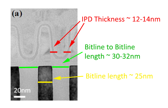
The inter poly dielectric (IPD) is the tricky part here -- because it wraps around every floating gate, the minimum distance between two floating gates (and hence bitlines) must be at least twice the thickness of the IPD. Scaling the IPD is difficult because if you make it too thin, the cell becomes vulnerable to leakage because the IPD won't be able to reliably insulate the floating gate. Generally it's considered impossible to scale the IPD below 10nm, so 26nm is already pretty good and 20nm is hitting the limits.
IMFT's approach is different. It's a high-k metal gate design and the wordline no longer needs to be wrapped around the floating gate, but I'm not going to go into more detail about that here. The short summary is that it allows for a symmetrical 20nm design without sacrificing reliability.
Courtesy of EETimes.com
In addition, you will want to have some conducting poly-silicon (i.e. wordline/control gate) between every bitline as well to build up capacitance, so in reality it's much harder scale the bitline length compared to the wordline. There is no wrapping issue with wordlines and the only thing you really have to take into account is wordline to wordline interference. To battle that, all NAND manufacturers are currently using tiny air gaps between every wordline to reduce the interference and still be able to scale down the NAND.
| IMFT (Intel/Micron) | Toshiba/SanDisk | |||
| NAND Process | 20nm 64Gbit | 20nm 128Gbit | 19nm 64Gbit (1st gen) | A19nm 64Gbit (2nd gen) |
| Cell Size | 20nm x 20nm | 19nm x 26nm | 19nm x 19.5nm | |
| Die Size | 118mm2 | 202mm2 | 113mm2 | 94mm2 |
| Gbit per mm2 | 0.542 | 0.634 | 0.566 | 0.681 |
With the second generation 19nm NAND, Toshiba/SanDisk has been able to cut the bitline length from 26nm to 19.5nm. It's still 19nm per marketing standards but at the engineering level this is pretty significant. Unfortunately the NAND is so new that I don't know what Toshiba/SanDisk has done to achieve a 19nm x 19.5nm cell size. It's certainly possible that Toshiba/SanDisk has also transitioned to a high-k metal gate process but we'll know more when the chip is put under a microscope.
It's interesting that while IMFT's 20nm NAND has smaller cell size than Toshiba's/SanDisk's first generation 19nm die, the density is still lower. I believe this has to do with IMFT's relatively poor memory area efficiency, which is only 52% for the 20nm 64Gbit die (i.e. 52% of the die is the actual memory part; the rest is peripheral circuits like interconnects and alike).
The real question for most users will be what sort of performance you can get out of the new NAND, however, so let's move on to benchmarks with the Plextor M6S/M6M.


30 Comments
View All Comments
Kristian Vättö - Friday, April 11, 2014 - link
Yes, there will be a review of the M6e. There has been some issues with testing and hence it's taking this long but it'll be my first priority as soon as we are able to overcome the issues.n3cw4rr10r - Thursday, April 10, 2014 - link
The prices for SSDs are still high imo. I am surprised they are still holding @ approx $1/gb in most cases.philipma1957 - Thursday, April 10, 2014 - link
samsung evo is far below $1 a gb and crucial M550's are far below $1 a gbssj3gohan - Thursday, April 10, 2014 - link
Finally actual proper idle power consumption results! It only took you a bit more than 5 years!HIPM and DIPM have been supported on all desktop systems - all desktop OSes as well as all hardware platforms - since the Athlon 64 X2 and first generation Core 2 (i945 chipset) times. I have been measuring SSD power consumption since they first came out - and yes, ever since the first SSDs, most of them supported the full gamut of power management - and have always been baffled that no review site on the internet has ever published accurate idle power consumption data. You are - aside from a few blogs I have come across - the first one. Congratulations!
Now, it's true that the first instances of especially DIPM were frought with latency issues and for a long time DIPM was turned off by default on Linux kernels (although Windows always forces it on in anything but the 'performance' power profile since Vista). Also, and this is probably the biggest issue, lots of BIOSes do not properly report SATA LPM or have it off by default. As it is usually fairly well hidden away it is not something many people think to turn on.
SATA ALPM is not at all a mobile feature. It has never been. Since support was baked in it has always been available to both laptop and desktop users. And with SSDs spending >>99% in idle, it represents easy and harmless power savings both in the SSD as well as the SATA I/O on the motherboard.
zodiacsoulmate - Thursday, April 10, 2014 - link
wow nice info!chubbypanda - Friday, April 11, 2014 - link
That's right. I always wondered why SSD reviewers at AnandTech claim it's mobile only. It's available at least on Denlow platform for sure.By the way, HIPM/DIPM feature itself is easy to control in Windows with simple registry update:
https://communities.intel.com/message/225489
Kristian Vättö - Friday, April 11, 2014 - link
"Also, and this is probably the biggest issue, lots of BIOSes do not properly report SATA LPM or have it off by default."That is the issue I had previously. The motherboard in my old testbed doesn't have the option to enable link power management and hence I couldn't perform those tests.
Ethos Evoss - Thursday, April 10, 2014 - link
Don't understand your tests ...It is all bollocks.. so few months back M5M was best and now it is on bottom ? that is all BULLCRAP
DanNeely - Thursday, April 10, 2014 - link
The M5M was reviewed a year ago. It's performance was underwhelming compared to sata drives then; but at the time getting an mSata drive at retail was much easier said than done; and at the time it was still a reasonable buy for its money. Since then much better mSata drives have came out and Plextor is trying to charge a premium device price while providing performance much worse than that of competing products that are significantly cheaper.http://anandtech.com/show/6722/plextor-m5m-256gb-m...
Ethos Evoss - Thursday, April 10, 2014 - link
Then M6M is NOT big step from M5M .. I have 2x M5M 256GB and they fliesI am not replacing then .. not worth ..