The iPhone 5s Review
by Anand Lal Shimpi on September 17, 2013 9:01 PM EST- Posted in
- Smartphones
- Apple
- Mobile
- iPhone
- iPhone 5S
A7 SoC Explained
I’m still surprised by the amount of confusion around Apple’s CPU cores, so that’s where I’ll start. I’ve already outlined how ARM’s business model works, but in short there are two basic types of licenses ARM will bestow upon its partners: processor and architecture. The former involves implementing an ARM designed CPU core, while the latter is the creation of an ARM ISA (Instruction Set Architecture) compatible CPU core.
NVIDIA and Samsung, up to this point, have gone the processor license route. They take ARM designed cores (e.g. Cortex A9, Cortex A15, Cortex A7) and integrate them into custom SoCs. In NVIDIA’s case the CPU cores are paired with NVIDIA’s own GPU, while Samsung licenses GPU designs from ARM and Imagination Technologies. Apple previously leveraged its ARM processor license as well. Until last year’s A6 SoC, all Apple SoCs leveraged CPU cores designed by and licensed from ARM.
With the A6 SoC however, Apple joined the ranks of Qualcomm with leveraging an ARM architecture license. At the heart of the A6 were a pair of Apple designed CPU cores that implemented the ARMv7-A ISA. I came to know these cores by their leaked codename: Swift.
At its introduction, Swift proved to be one of the best designs on the market. An excellent combination of performance and power consumption, the Swift based A6 SoC improved power efficiency over the previous Cortex A9 based design. Swift also proved to be competitive with the best from Qualcomm at the time. Since then however, Qualcomm has released two evolutions of its CPU core (Krait 300 and Krait 400), and pretty much regained performance leadership over Apple. Being on a yearly release cadence, this is Apple’s only attempt to take back the crown for the next 12 months.
Following tradition, Apple replaces its A6 SoC with a new generation: A7.
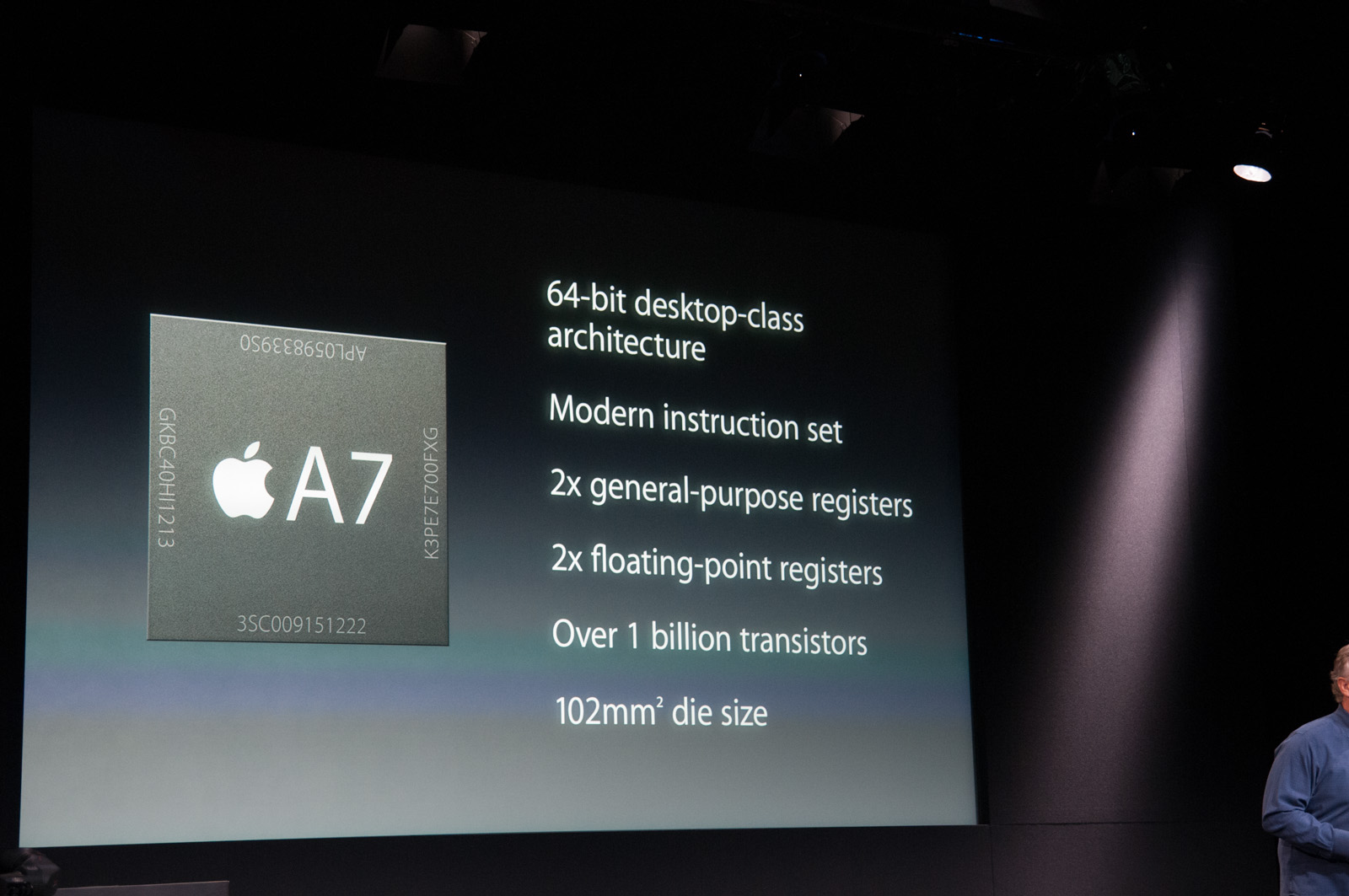
With only a week to test battery life, performance, wireless and cameras on two phones, in addition to actually using them as intended, there wasn’t a ton of time to go ridiculously deep into the new SoC’s architecture. Here’s what I’ve been able to piece together thus far.
First off, based on conversations with as many people in the know as possible, as well as just making an educated guess, it’s probably pretty safe to say that the A7 SoC is built on Samsung’s 28nm HK+MG process. It’s too early for 20nm at reasonable yields, and Apple isn’t ready to move some (not all) of its operations to TSMC.
The jump from 32nm to 28nm results in peak theoretical scaling of 76.5% (the same design on 28nm can be no smaller than 76.5% of the die area at 32nm). In reality, nothing ever scales perfectly so we’re probably talking about 80 - 85% tops. Either way that’s a good amount of room for new features.
At its launch event Apple officially announced both die size for the A7 (102mm^2) as well as transistor count (over 1 billion). Don’t underestimate the magnitude of both of these disclosures. The technical folks at Cupertino are clearly winning some battle to talk more about their designs and not less. We’re not yet at the point where I’m getting pretty diagrams and a deep dive, but it’s clear that Apple is beginning to open up more (and it’s awesome).
Apple has never previously disclosed transistor count. I also don’t know if this “over 1 billion” figure is based on a schematic or layout transistor count. The only additional detail I have is that Apple is claiming a near doubling of transistors compared to the A6. Looking at die sizes and taking into account scaling from the process node shift, there’s clearly a more fundamental change to the chip’s design. It is possible to optimize a design (and transistors) for area, which seems to be what has happened here.
The CPU cores are, once again, a custom design by Apple. These aren’t Cortex A57 derivatives (still too early for that), but rather some evolution of Apple’s own Swift architecture. I’ll dive into specifics of what I’ve been able to find in a moment. To answer the first question on everyone’s mind, I believe there are two of these cores on the A7. Before I explain how I arrived at this conclusion, let’s first talk about cores and clock speeds.
I always thought the transition from 2 to 4 cores happened quicker in mobile than I had expected. Thankfully there are some well threaded apps that have been able to take advantage of more than two cores and power gating keeps the negative impact of the additional cores down to a minimum. As we saw in our Moto X review however, two faster cores are still better for most uses than four cores running at lower frequencies. NVIDIA forced everyone’s hand in moving to 4 cores earlier than they would’ve liked, and now you pretty much can’t get away with shipping anything less than that in an Android handset. Even Motorola felt necessary to obfuscate core count with its X8 mobile computing system. Markets like China seem to also demand more cores over better ones, which is why we see such a proliferation of quad-core Cortex A5/A7 designs. Apple has traditionally been sensible in this regard, even dating back to core count decisions in its Macs. I remembering reviewing an old iMac and pitting it against a Dell XPS One at the time. This was in the pre-power gating/turbo days. Dell went the route of more cores, while Apple chose for fewer, faster ones. It also put the CPU savings into a better GPU. You can guess which system ended out ahead.
In such a thermally constrained environment, going quad-core only makes sense if you can properly power gate/turbo up when some cores are idle. I have yet to see any mobile SoC vendor (with the exception of Intel with Bay Trail) do this properly, so until we hit that point the optimal target is likely two cores. You only need to look back at the evolution of the PC to come to the same conclusion. Before the arrival of Nehalem and Lynnfield, you always had to make a tradeoff between fewer faster cores and more of them. Gaming systems (and most users) tended to opt for the former, while those doing heavy multitasking went with the latter. Once we got architectures with good turbo, the 2 vs 4 discussion became one of cost and nothing more. I expect we’ll follow the same path in mobile.
Then there’s the frequency discussion. Brian and I have long been hinting at the sort of ridiculous frequency/voltage combinations mobile SoC vendors have been shipping at for nothing more than marketing purposes. I remember ARM telling me the ideal target for a Cortex A15 core in a smartphone was 1.2GHz. Samsung’s Exynos 5410 stuck four Cortex A15s in a phone with a max clock of 1.6GHz. The 5420 increases that to 1.7GHz. The problem with frequency scaling alone is that it typically comes at the price of higher voltage. There’s a quadratic relationship between voltage and power consumption, so it’s quite possibly one of the worst ways to get more performance. Brian even tweeted an image showing the frequency/voltage curve for a high-end mobile SoC. Note the huge increase in voltage required to deliver what amounts to another 100MHz in frequency.
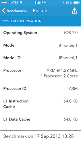
The combination of both of these things gives us a basis for why Apple settled on two Swift cores running at 1.3GHz in the A6, and it’s also why the A7 comes with two cores running at the same max frequency. Interestingly enough, this is the same max non-turbo frequency Intel settled at for Bay Trail. Given a faster process (and turbo), I would expect to see Apple push higher frequencies but without those things, remaining conservative makes sense. I verified frequency through a combination of reporting tools and benchmarks. While it’s possible that I’m wrong, everything I’ve run on the device (both public and not) points to a 1.3GHz max frequency.
Verifying core count is a bit easier. Many benchmarks report core count, I also have some internal tools that do the same - all agreed on the same 2 cores/2 threads conclusion. Geekbench 3 breaks out both single and multithreaded performance results. I checked with the developer to ensure that the number of threads isn’t hard coded. The benchmark queries the max number of logical CPUs before spawning that number of threads. Looking at the ratio of single to multithreaded performance on the iPhone 5s, it’s safe to say that we’re dealing with a dual-core part:
| Geekbench 3 Single vs. Multithreaded Performance - Apple A7 | ||||||
| Integer | FP | |||||
| Single Threaded | 1471 | 1339 | ||||
| Multi Threaded | 2872 | 2659 | ||||
| A7 Advantage | 1.97x | 1.99x | ||||
| Peak Theoretical 2C Advantage | 2.00x | 2.00x | ||||
Now the question is, what’s changed in these cores?


464 Comments
View All Comments
MatthiasP - Tuesday, September 17, 2013 - link
Wow, first real review on the web AND deep as always, a very nice job from Anand. :)sfaerew - Wednesday, September 18, 2013 - link
Benchmarks(GFXBench 2.7,3DMark.Basemark X.etc.) are AArch64 version?There are 30~40% performance gap between v32geekbench and v64geekbench.
INT(ST)1471 vs 1065.
FP(ST)1339 vs 983
Wilco1 - Wednesday, September 18, 2013 - link
And Bay Trail Geekbench at 2.4GHz: 1063 (INT), 866 (FP)So A7 has beaten BT already by a huge margin despite BT not even being for sale yet...
TraderHorn - Wednesday, September 18, 2013 - link
You're comparing 64bit A7 vs 32bit BT. The 32bit #s are dead even. It'll be interesting to see if BT gets a similar performance boost when Win8 64bit versions are released in 1h 2014.Wilco1 - Wednesday, September 18, 2013 - link
BT's 32-bit result includes hardware accelerated AES, which skews its score (without it, its score is ~936). The 64-bit A7 result does also use hardware acceleration, so it is more comparable.Yes BT will get a speedup from 64-bit as well, but won't be nearly as much as A7 gets: its 32-bit result already has the AES acceleration, and x64 nearly isn't as different from x86 as A64 is from A32.
However the interesting things is that not even in 32-bit A7 wins by a good margin, but that it wins despite running at almost half the frequency of Bay Trail... Forget about Bay Trail, this is Haswell territory - the MacBook Air with the 15W 3.3GHz i7-4650U scores 3024 INT and 3003 FP.
Now imagine a quad core tablet/laptop version of the A7 running at 2GHz on TSMC 20nm next year.
smartypnt4 - Wednesday, September 18, 2013 - link
Why does the frequency matter? If the TDP of the chips are similar (Bay Trail was tested and verified by Anand as using 2.5W at the SoC level under load), who gives a flip about the frequency?If Apple wanted to double the frequency of the chip, they'd need something on the order of 4x the amount of power it already consumes (assuming a back-of-the-napkin quadratic relationship, which is approximately correct), putting it at ~6-8W or so at full load. That's assuming such a scaling could even be done, which is unlikely given that Apple built the thing to run at 1.3GHz max. You can't just say "oh, I want these to switch faster, so let's up the voltage." There's more that goes in to the ability to scale voltage than just the process node you're on.
Now, I will agree that this does prove that if Apple really wanted to, they could build something to compete with Haswell in terms of raw throughput. Next year's A8 or whatever probably will compete directly with Haswell in raw theoretical integer and FP throughput, if Apple manages to double performance again. That's not a given since they had to use ~50% more transistors to get a performance doubling from the A6 to the A7, and building a 1.5B transistor chip is nontrivial since yields are inversely proportional to the number of transistors you're using.
Next year will be really interesting, though. What with Apple's next stuff, Broadwell, the first A57 designs, Airmont, and whatever Qualcomm puts out (haven't seen anything on that, which is odd for Qualcomm.)
Wilco1 - Wednesday, September 18, 2013 - link
Frequency & process matters. Current phones use about 2W at max load without the screen (see recent Nexus 7 test), so the claimed 2.5W just for BT is way too much for a phone. That means (as you explained) it must run at a lower frequency and voltage to get into phones - my guess we won't see anything faster than the Z3740 with a max clock of 1.8GHz. Therefore the A7 will extend its lead even further.According to TSMC 20nm will give a 30% frequency boost at the same power. So I'd expect that a 2GHz A7 would be possible on 20nm using only 35% more power. That means the A7 would get 75% more performance at a small cost in power consumption. This is without adding any extra transistors.
Add some tweaks (like faster memory) and such a 2GHz A7 would be similar in performance as the 15W Haswell in MacBook Air. So my point is that with a die shrink and a slight increase in power they already have a Haswell competitor.
smartypnt4 - Wednesday, September 18, 2013 - link
Frequency and process matter in that they affect power consumption. If Intel can get Bay Trail to do 2.4GHz on something like 1.0V, then the power should be fine. Current Haswell stuff tops out its voltage around 1.1V or so in laptops (if memory serves), so that's not unreasonable.All of this assumes Geekbench is valid for comparing HSW on Win8 to ARMv8/Cyclone on iOS, which I have serious reservations about attempting to do.
The other issue I have is this: you're talking about a 50% clock boost giving a 100% increase in performance if we look at the Geekbench scores. That's simply not possible. Had you said "raise the clock to 1.6-1.7GHz and give it 4 cores," I'd be right behind you in a 2x theoretical performance increase. But a 50% clock boost will never yield a 100% increase with the same core, even if you change the memory controller.
Also, somehow your math doesn't add up for power... Are you hypothesizing that a 2GHz A7 (with 75% of the performance of Haswell 15W, not the same - as per Geekbench) can pull 2.6W while Haswell needs 15W to run that test? Granted, Haswell integrates things that the A7 doesn't. Namely, more advanced I/O (PCIe, SATA, USB, etc.), and the PCH. Using very fuzzy math, you can claim all of that uses 1/2 the power of the chip.
That brings Haswell's power for compute down to 7-8W, more or less. And you're going to tell me that Apple has figured out how to get 75% of the performance of a 7W part in 2.6W, and Intel hasn't? Both companies have ~100k employees. One is working on a ton of different stuff, and one makes processors, basically exclusively (SSDs and WiFi stuff too, but processors is their main drive). You're telling me that a (relatively) small cadre of guys at Apple have figured out how to do it, and Intel hasn't done it yet on a part that costs ~6x as much after trying to get deep into the mobile space for years. I find that very hard to believe.
Even with the 14nm shrink next year, you're talking about a 30% power savings for Intel's stuff. That brings the 15W total down to 10.5W, and the (again, super, ridiculously fuzzy) computing power to ~5-6W. On a full node smaller than what Apple has access to. And you're saying they'd hypothetically compete in throughput with a 2.6W part. I'm not sure I believe that.
Then again, I suppose theoretical bandwidth could be competitive. That's simply a factor of your peak IPC, not your average IPC while the device is running. I don't know enough about the low level architecture of the A7 (no one does), so I'll just leave it here I guess.
I'm gonna go now... I'm starting to reason in circles.
Wilco1 - Wednesday, September 18, 2013 - link
The sort of "simple" tweaks I was thinking of are: an improved memory controller and prefetcher, doubling of L2, larger branch predictor tables. Assuming a 30% gain due to those tweaks, the result is a 100% speedup at 2GHz (1.3 to 2.0 GHz is a 54% speedup, so you get 1.54 * 1.3 = 2.0x perf). The 30% gain due to tweaks is pure speculation of course, however NVidia claims 15-30% IPC gain for similar tweaks in Tegra 4i, so it's not entirely implausible. As you say a much simpler alternative would be just to double the cores, but then your single threaded performance is still well below that of Haswell.You can certainly argue some reduction in the 15W TDP of Haswell due to IO, however with Turbo it will try to use most of that 15W if it can (the Air goes up to 3.3GHz after all).
Yes I am saying that a relative newcomer like Apple can compete with Intel. Intel may be large, but they are not infallible, after all they made the P4, Itanium and Atom. A key reason AMD cited for moving into ARM servers was that designing an ARM CPU takes far less effort than an equivalent performing x86 one. So the ISA does still matter despite some claiming it no longer does.
smartypnt4 - Wednesday, September 18, 2013 - link
My point wasn't that Apple can't compete; far from it. If anything, the A7 shows they can compete for the most part. However, what you suggest is that Apple could theoretically have the same performance as Intel on a full node process larger at half the power. Ihave no illusions that Intel is infallible. Stuff like Larrabee and the underwhelming GPU in Bay Trail prove that they aren't. I just seriously doubt that Apple could beat Intel at its own game. Specifically, in CPU performance, which is an area it's dominated for years. It's possible, but I find it relatively unlikely, especially this early in Apple's lifetime as a chip designer.
On a different note, after looking at the Geekbench results more, I feel like it's improperly weighted. The massive performance improvement in AES and SHA encryption may be skewing the overall result... I need to dig more in to Geekbench before coming to an actual conclusion. I'm also still not convinced that comparing cross-platform results is actually valid. I'd like to believe it is, but I've always had reservations about it.