Samsung’s 3D Vertical NAND Set to Improve NAND Densities
by Jarred Walton on August 6, 2013 6:12 PM EST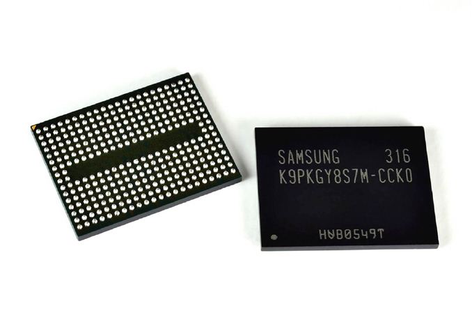
Ars Technica has posted information on Samsung’s new 3D Vertical NAND technology, and it promises to boost densities for SSDs and other similar devices dramatically. Samsung announced last night that they have begun mass production of the devices.
Using up to 24 vertical NAND elements, Samsung predicts that they will be able to scale up to 1Tb per individual NAND chip. It’s not clear exactly how large the initial chips will be, but with conventional 19nm NAND currently shipping in 128Gb capacities we’d expect at least two to four times as much storage per chip. That means using current SSD standards of eight channels of NAND we’d see capacities for “commodity” SSDs move from 128GB to 256GB or even 512GB, and with four NAND die per package we could easily hit 2TB SSDs. The days of needing a secondary storage device with a hard drive could be quickly coming to a close depending on the timing and pricing.
There’s a second technology also coming into play with V-NAND that addresses concerns with reliability and longevity of NAND. Rather than storing charge in a set of floating gate transistors, with voltage levels corresponding to either 0/1 (SLC), 00/01/10/11 (MLC), or 000/001/010/011/100/101/110/111 (TLC), V-NAND will use Charge Trap Flash (CTF). Samsung states, “With Samsung's CTF-based NAND flash architecture, an electric charge is temporarily placed in a holding chamber of the non-conductive layer of flash that is composed of silicon nitride (SiN), instead of using a floating gate to prevent interference between neighboring cells.” Samsung claims that at a minimum CTF will have at least 2x the lifespan of floating gate NAND, and potentially as much as a 10x increase. Write performance is also doubled relative to conventional 10nm-class floating gate NAND.
Sadly, there’s no specific word on availability or pricing right now, and historically with V-NAND just entering mass production we’re likely a year or more away from production SSDs using the technology. Samsung is obviously a major player in both the NAND and SSD markets, so Samsung SSDs using V-NAND are inevitable, but testing and validation will certainly require some time. Hopefully this all comes sooner rather than later, though, as the potential to ditch conventional storage and get improved performance and reliability compared to current NAND seems like the perfect storm needed to end our reliance on slow, spinning platters.
Source: Ars Technica


33 Comments
View All Comments
lmcd - Tuesday, August 6, 2013 - link
Hopefully this ends up desirably priced. It'd be great to see SSD storage overtake Disk for mainstream and value desktop, laptop storage by three years from now.Vigneshj - Tuesday, August 6, 2013 - link
Having entered into mass production mode, doesn't that mean significant portion of Validation & testing is completed already? (forgive me, noob question!)coder543 - Tuesday, August 6, 2013 - link
Exactly. Mass production is a different scale than what the article describes, at least to me. If this isn't on the market in six months, someone is using a weird definition for mass production.lilmoe - Tuesday, August 6, 2013 - link
I agree. Since these chips should be cheaper to produce (smaller process), while holding a significantly greater amount of data, and having at least 2x more reliability, the only reason to delay release of these chips would probably be to get rid of the current stock of SSDs.If the info holds true, I believe current SSDs will render obsolete in price, performance, and capacity. This should also be really bad news for conventional spinning drives.
All depends on pricing though. I don't believe Samsung is stupid enough to sell those for cheap, at least not till they make a good margin on them if they get market lead.
JarredWalton - Tuesday, August 6, 2013 - link
Just because you're producing the NAND (or V-NAND) doesn't mean it's going into fully functional products, let along SSDs. Once the NAND is being mass produced, someone needs to integrate that into a useful product. We might see simple flash drives, SD/Micro SD type devices, etc. at first followed by the integration of the product into a fully functional SSD. That last one is a big step, though, as it needs controller logic, testing, validation, debugging, etc. which is why I think this could be more like 1-2 years out.Also, 10nm is very cutting edge, unless Samsung is somehow using a different definition than others. IMFT is on 19nm I think, and Intel's CPU stuff is still at 22nm with 14nm coming next year followed by 10nm probably in three years. NAND is easier to manufacture (well, test and validate at least) is my understanding, which is why most first wafers off a new assembly line are NAND wafers. When did the first 1xnm NAND start mass production vs. when did it show up in the first consumer SSDs? I'd say a year at least passed.
Anyway, we'll see what happens. I for one would love to pay twice the cost of HDD storage to get an SSD of similar capacity, where right now it's more like 10x the cost for the same storage capacity. I'm looking forward to the day where I can run a 1TB SSD and not have it cost as much as the CPU, GPU, and motherboard combined.
p1esk - Tuesday, August 6, 2013 - link
Samsung has not disclosed the process size. Where did 10nm info came from?http://www.samsung.com/global/business/semiconduct...
JarredWalton - Tuesday, August 6, 2013 - link
From Ars Technica...looks like they misinterpreted something in the document. Editing...garadante - Tuesday, August 6, 2013 - link
I think it's just a common misinterpretation for people to read 10 nm class devices as 10 nm devices. 10 nm class is anything from 10-19 nm, and when they say 10 nm class devices, they typically mean the process is actually 19 nm and they're just trying to make it seem more incredible and ahead of the competition than it really is. Woohoo, marketing lingo.Mondozai - Wednesday, August 7, 2013 - link
"From Ars Technica...looks like they misinterpreted something in the document. Editing..."The danger of blindly re-writing somene else's news post.
JarredWalton - Wednesday, August 7, 2013 - link
Thanks for that...that was highly useful. There was no "blind rewriting" involved, thanks. It was a minor error that has been corrected, based on their use of "10nm-class" vs. "10nm".