The ARM Diaries, Part 2: Understanding the Cortex A12
by Anand Lal Shimpi on July 17, 2013 12:30 PM EST- Posted in
- CPUs
- Arm
- SoCs
- Cortex A12
A couple of weeks ago I began this series on ARM with a discussion of the company’s unique business model. In covering semiconductor companies we’ve come across many that are fabless, but it’s very rare that you come across a successful semiconductor company that doesn’t even sell a chip. ARM’s business entirely revolves around licensing IP for its instruction set as well as its own CPU (and now GPU and video) cores.
Before we get into discussions of specific cores, it’s important to talk about ARM’s portfolio as a whole. In the PC space we’re used to focusing on Intel’s latest and greatest microarchitectures, which are then scaled in various ways to hit lower price targets. We might see different core counts, cache sizes, frequencies and maybe even some unfortunate instruction set tweaking but for the most part Intel will deliver a single microarchitecture to cover the vast majority of the market. These days, this microarchitecture is simply known as Core.
Back in 2008, Intel introduced a second microarchitecture under the Atom brand to target lower cost (and lower power) markets. The combination of Atom and Core spans the overwhelming majority of the client computing market for Intel. The prices of these CPUs range from the low double digits with Atom to many hundreds of dollars for the highest end Core processors (the most expensive desktop Haswell is $350, however mobile now extends up to $1100). There are other designs that target servers (which are then repurposed for ultra high-end desktops), but those are beyond the scope of this discussion for now.
If we limit our discussion to personal computing devices (smartphones, tablets, laptops and desktops), where Intel uses two microarchitectures ARM uses three. The graphic below illustrates the roadmap:
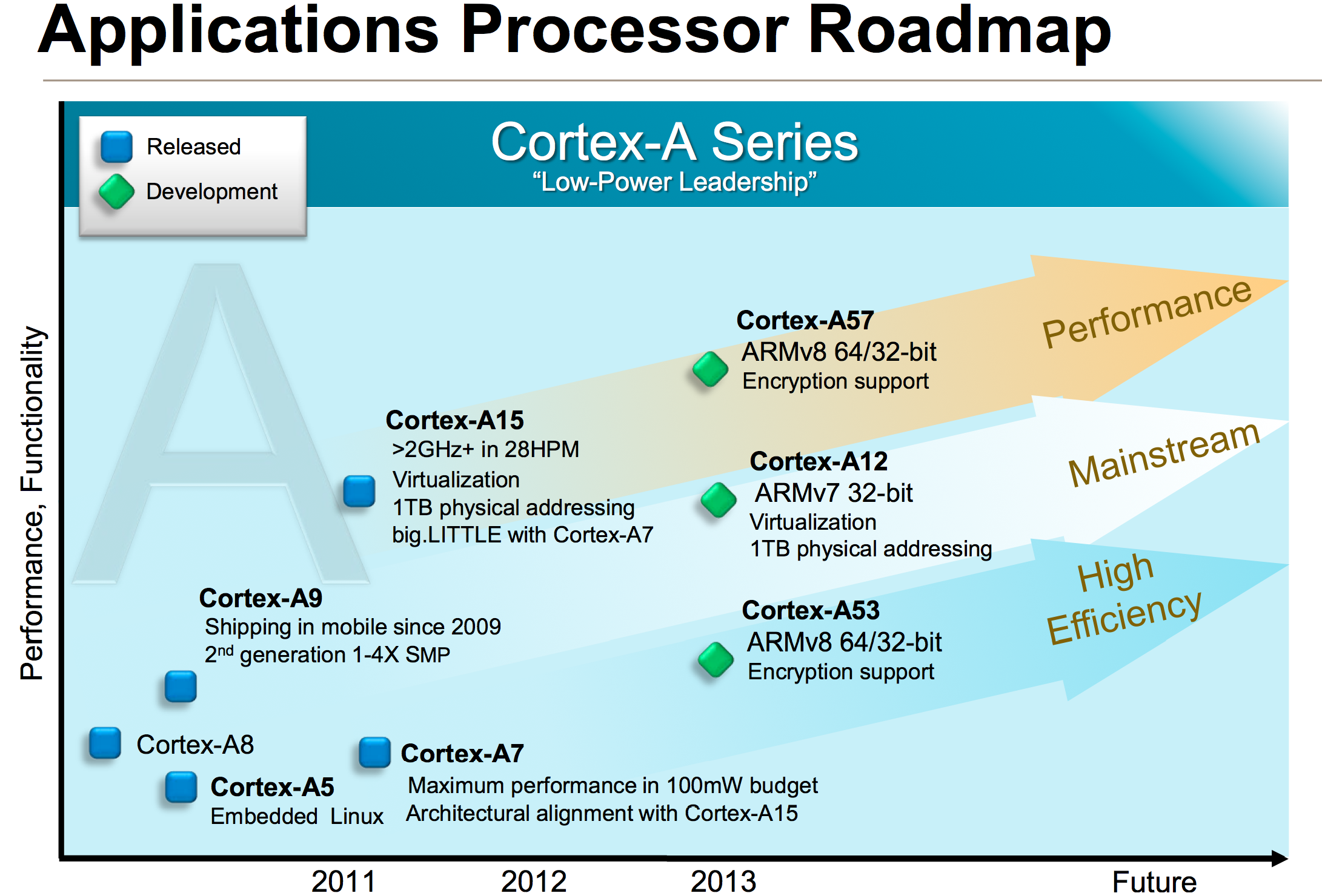
You need to somewhat ignore the timescale on the x-axis since those dates really refer to when ARM IP is first available to licensees, not when products are shipping to consumers, but you get an idea for the three basic vectors of ARM’s Cortex A-series of processor IP. Note that there are also Cortex R (embedded) and Cortex M (microcontroller) series of processor IP offered as well, but once again those are beyond the scope of our discussion here.
If we look at currently available cores, there’s the Cortex A15 on the high end, Cortex A9 for the mainstream and Cortex A7 for entry/low cost markets. If we’re to draw parallels with Intel’s product lineup, the Cortex A15 is best aligned with ultra low power/low frequency Core parts (think Y-series SKUs), while the Cortex A9 vector parallels Atom. Cortex A7 on the other hand targets a core size/cost/power level that Intel doesn’t presently address. It’s this third category labeled high efficiency above that Intel doesn’t have a solution for. This answers the question of why ARM needs three microarchitectures while Intel only needs two: in mobile, ARM targets a broader spectrum of markets than Intel.
Dynamic Range
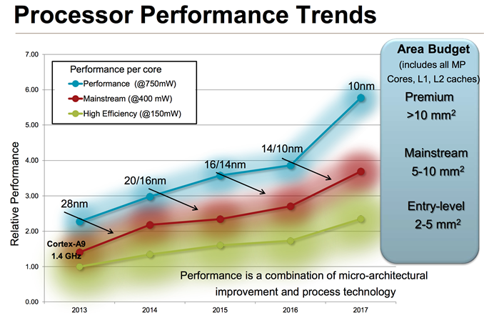
If you’ve read any of our smartphone/tablet SoC coverage over the past couple of years you’ll note that I’m always talking about an increasing dynamic range of power consumption in high-end smartphones and tablets. Each generation performance goes up, and with it typically comes a higher peak power consumption. Efficiency improvements (either through architecture, process technology or both) can make average power in a reasonable workload look better, but at full tilt we’ve been steadily marching towards higher peak power consumption regardless of SoC vendor. ARM provided a decent overview of the CPU power/area budget as well as expected performance over time of its CPU architectures:

Looking at the performance segment alone, we’ll quickly end up with microarchitectures that are no longer suited for mobile, either because they’re too big/costly or they draw too much power (or both).
The performance vector of ARM CPU IP exists because ARM has its sights set higher than conventional smartphones. Starting with the Cortex A57, ARM hopes to have a real chance in servers (and potentially even higher performance PCs, Windows RT and Chrome OS being obvious targets).
Although we see limited use of ARM’s Cortex A15 in smartphones today (some international versions of the Galaxy S 4), it’s very clear that for most phones a different point on the power/performance curve makes the most sense.
The Cortex A8 and A9 were really the ARM microarchitectures that drove smartphone performance over the past couple of years. The problem is that while ARM’s attentions shifted higher up the computing chain with Cortex A15, there was no successor to take the A9’s place. ARM’s counterpoint would be that Cortex A15 can be made suitable for lower power operation, however its partners (at least to date) seemed to be focused on extracting peak performance from the A15 rather than pursuing a conservative implementation designed for lower power operation. In many ways this makes sense. If you’re an SoC vendor that’s paying a premium for a large die CPU, you’re going to want to get the most performance possible out of the design. Only Apple seems to have embraced the idea of using die area to deliver lower power consumption.
The result of all of this is that the Cortex A9 needed a successor. For a while we’d been hearing about a new ARM architecture that would be faster than Cortex A9, but lower power (and lower performance) than Cortex A15. Presently, the only architecture in between comes from Qualcomm in the form of some Krait derivative. For ARM to not let its IP licensees down, it too needed a solution for the future of the mainstream smartphone market. Last month we were introduced to that very product: ARM’s Cortex A12.
Slotting in numerically between A9 and A15, the initial disclosure unfortunately didn’t come with a whole lot of actual information. Thankfully, we now have some color to add.


65 Comments
View All Comments
wumpus - Friday, July 19, 2013 - link
And I didn't see anyway for 32bit ARM to access more than 3G. Maybe there is, but the PAE-style mechanism that allowed each process to access 4G of ram (well 2-3G of user space and 2-1G of OS space). It looks like each process sees 32 bit MMU tags meaning no way to access the whole RAM. Again, somewhere in there they might have an unholy kludge, but I suspect that they are more than willing to do things the [PAE] intel way [not the 286 way that Microsoft forced everyone to support a decade after it was consigned to the junkyard].wumpus - Friday, July 19, 2013 - link
So how does one process access more than 4G (3G if Linux, likely less else where)? There is a reason nobody uses 32 bit chips. If you really looked up the datasheets, the *80386* chip could access way more than 64G virtual ram (it didn't have the pins for more than 4G of memory). You could even access it fairly easily in a process, but as far as I know *nobody* ever tried that.Note: Linux 0.x and I think 1.x could both handle 3G per memory process. Maybe not, I know Linus used the 386 segmentation scheme natively on different processes, but I have no idea if the 386 MMU could handle tags that depended on the segmentation scheme (it was quite possible you could either go wild with segments, or use them traditionally and have full MMU operation. I haven't looked at this stupid idea since 1990, when I learned the disaster that is x86.
We use 64 bit chips for a reason. If we didn't need to access memory the size of an integer register, I would strongly suspect that all integer registers would be 16 bits long (note the pentium4 computed integer operations 16 bits at a time, they are notably faster). Using a 64 bit register and 64 bit addressing means that you can access an entire database of arbitrary size (2^63, whatever that is), while using 32 bit machines requires a "networking" OS call to whichever process happens to have that particular datum in memory. It is yet another unholy kludge and the reason that "the only fatal mistake a computer architecture can have is too small a word size".
Wilco1 - Friday, July 19, 2013 - link
You don't need to access more than 3GB per process on a mobile! Mobiles/tablets will have 4GB of RAM, however each process still has it's own 32-bit address space and uses only a portion of the available RAM.There is no need to be so obsessed about 64-bit, you know the the Windows world is still mostly 32-bit 10 years after the introduction of Athlon64... Even Windows 8 still has a 32-bit version. So while there are lots of 64-bit chips around, most run only 32-bit code. My Athlon64 which I retired last year never ever ran 64-bit code during its entire life!
You only really require 64-bit addressing if you have big applications that need more than 3GB per process. Such applications are rare (your database is an example) and they only run on large expensive servers, not on mobiles. So clearly the need for 64-bit is extremely small, and mobiles/tablets will simply use PAE rather than switch to 64-bit for the foreseeable future.
Calinou__ - Saturday, July 20, 2013 - link
64 bit is still a technogy of the future. Not to mention PAE can be quite buggy sometimes, especially when running eg. proprietary drivers.Wolfpup - Thursday, July 25, 2013 - link
The timing on this seems weird. Didn't they know they needed a smaller jump between A9 and A15 years ago? I HOPE it's not really needed by late 2014/2015...I mean I hope by then we're all using A15, and maybe A5x or whatever... Or AMD's low power chips and SIlvermont!