The Haswell Review: Intel Core i7-4770K & i5-4670K Tested
by Anand Lal Shimpi on June 1, 2013 10:00 AM ESTDie Size and Transistor Count
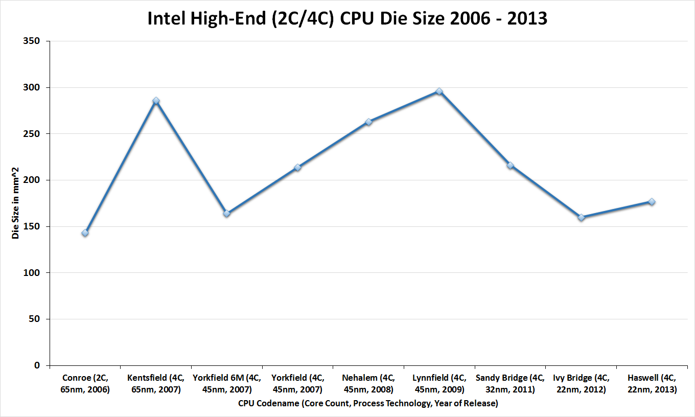
Moving on to die sizes and transistor counts, this year Intel is striving to be more straightforward and accurate than was the case with Sandy Bridge and Ivy Bridge. With the Bridge generation we didn’t initially get comparable numbers, only for the correction to throw in additional confusion. For Haswell Intel is laying things out from the start, listing both possible numbers so that either can be compared.
| CPU Specification Comparison | |||||||||
| CPU | Manufacturing Process | Cores | GPU | Transistor Count (Schematic) | Die Size | ||||
| Haswell GT3 4C | 22nm | 4 | GT3 | ? | 264mm2 (est) | ||||
| Haswell GT2 4C | 22nm | 4 | GT2 | 1.4B | 177mm2 | ||||
| Haswell ULT GT3 2C | 22nm | 2 | GT3 | 1.3B | 181mm2 | ||||
| Intel Ivy Bridge 4C | 22nm | 4 | GT2 | 1.2B | 160mm2 | ||||
| Intel Sandy Bridge E 6C | 32nm | 6 | N/A | 2.27B | 435mm2 | ||||
| Intel Sandy Bridge 4C | 32nm | 4 | GT2 | 995M | 216mm2 | ||||
| Intel Lynnfield 4C | 45nm | 4 | N/A | 774M | 296mm2 | ||||
| AMD Trinity 4C | 32nm | 4 | 7660D | 1.303B | 246mm2 | ||||
| AMD Vishera 8C | 32nm | 8 | N/A | 1.2B | 315mm2 | ||||
The two numbers for the most common Haswell configuration, Haswell GT2 4C, are 1.4 billion schematic transistors and 1.6 billion layout transistors. Why and what is the difference? The former count is the number of transistors in the schematic (hence the name), and is generally the number we go by when quoting transistor counts. Meanwhile the second number, the layout number, is the number of transistors used in the fabrication process itself. The difference comes from the fact that while the schematic will use one large transistor – being a logical diagram – production will actually use multiple transistors laid out in parallel for layout and process reasons. So how many transistors does Haswell have? It has both 1.4B and 1.6B, depending on which number we’re after, with 1.4B being the number Intel is passing around.
In any case, even among quad cores Haswell is going to come in a couple of different sizes. Along with the 1.4B transistor, 177mm2 4C/GT2 version of Haswell, there is the 4C/GT3 version of Haswell, which Intel doesn’t list the die size or transistor count for. Based on our rough measurements of the physical die we’re at 264mm2, which including the epoxy covering the die will run a bit large.
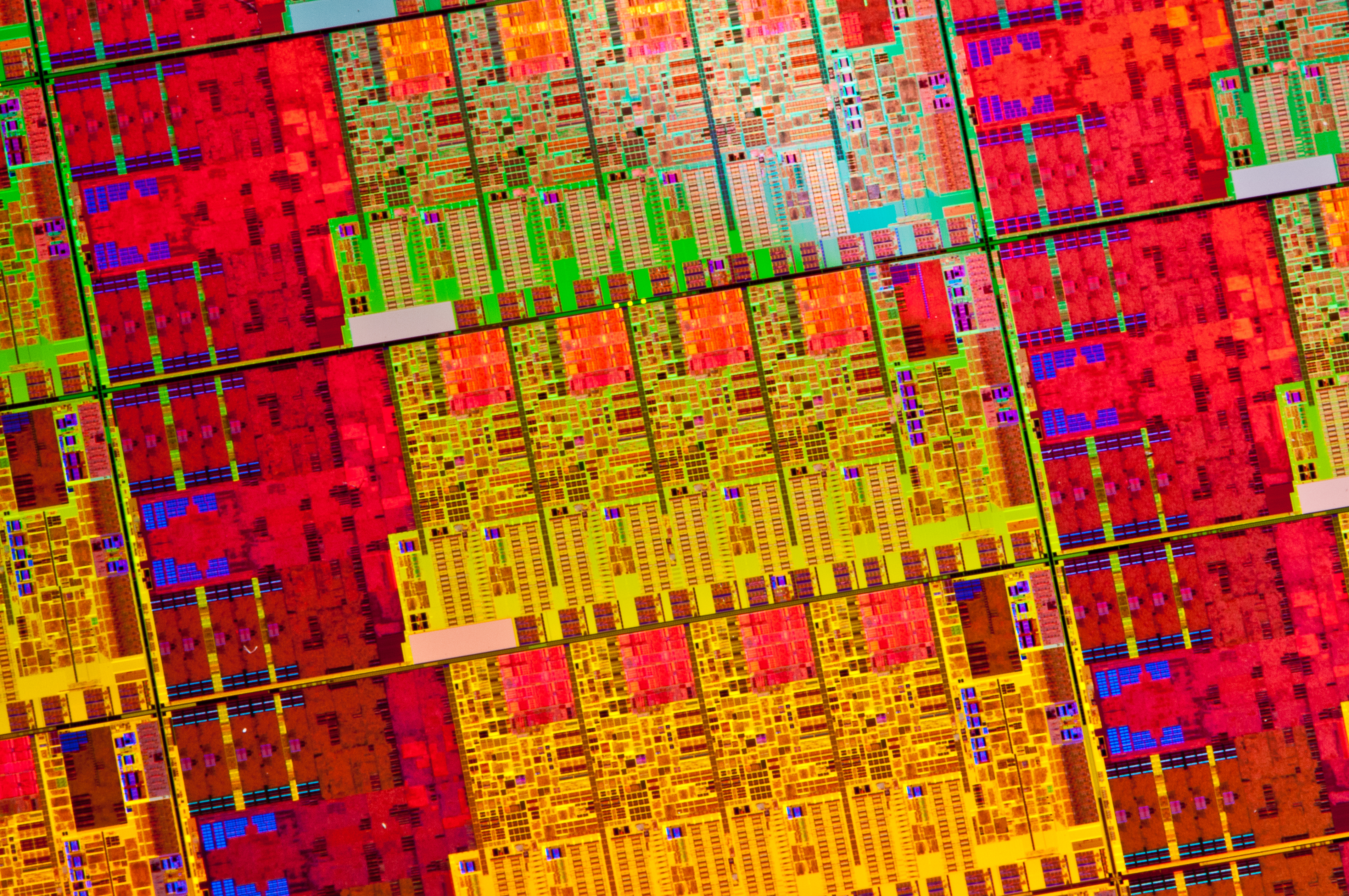
Breaking things down to the GPU portion of Haswell, based in turn on these measurements I came up with an 87mm^2 adder for the extra hardware in Haswell GT3 vs. GT2. Doubling that 87mm^2 we get a rough idea of how big the full 40 EU Haswell GPU might be: 174mm^2. If my math is right, this means that in a quad-core Haswell GT3 die, around 65% of the die area is GPU. This is contrary to the ~33% in a quad-core Haswell GT2. I suspect a dual-core + GT3 design is at least half GPU. Meanwhile Crystalwell, the 128MB eDRAM, adds another 84mm2 die (by our measurements) to the entire package.
On a comparative basis, the 4C/GT2 version of Haswell is roughly 200M transistors and 17mm2 bigger than the comparable 4C/GT2 version of Ivy Bridge. The transistor count increase is roughly what we’d expect, with most of those transistors going to Haswell itself while the GPU remains relatively unchanged. Though it’s interesting to note that while this marks a 17% increase in transistors, it’s only an 11% increase in die size. Ivy Bridge was a small die for an Intel, and while Haswell grows larger in exchange for the additional functionality the new architecture provides, it’s still a fairly small GPU and reaches a density greater than Ivy Bridge itself. Or to put this another way, Intel’s last tock CPU, Sandy Bridge, was larger still by almost 40mm2. It’s only once we start adding the relatively big GT3 GPU, and not the CPU, that we see Intel go well above 200mm2.


210 Comments
View All Comments