Intel Iris Pro 5200 Graphics Review: Core i7-4950HQ Tested
by Anand Lal Shimpi on June 1, 2013 10:01 AM ESTAddressing the Memory Bandwidth Problem
Integrated graphics solutions always bumped into a glass ceiling because they lacked the high-speed memory interfaces of their discrete counterparts. As Haswell is predominantly a mobile focused architecture, designed to span the gamut from 10W to 84W TDPs, relying on a power-hungry high-speed external memory interface wasn’t going to cut it. Intel’s solution to the problem, like most of Intel’s solutions, involves custom silicon. As a owner of several bleeding edge foundries, would you expect anything less?
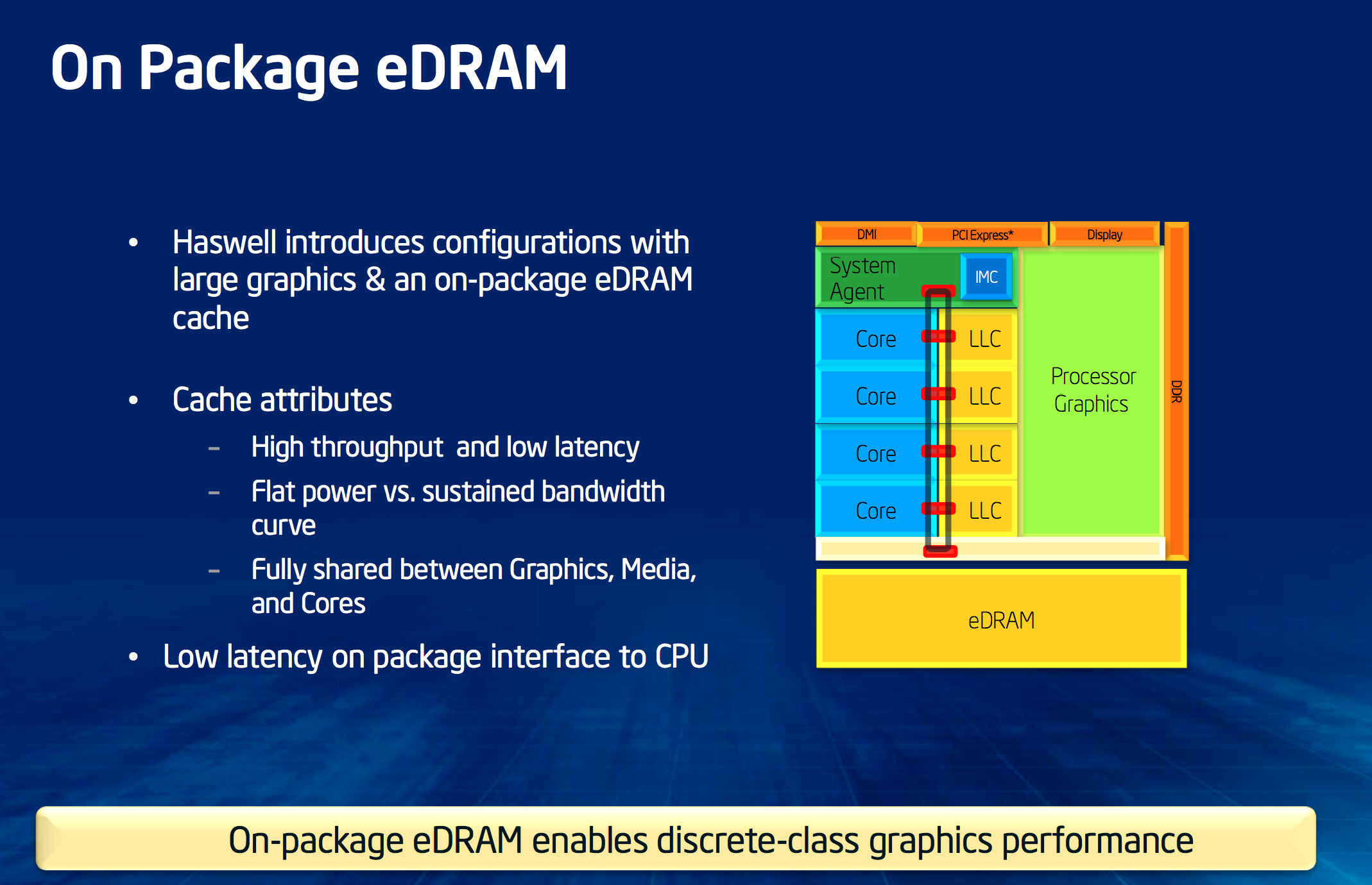
As we’ve been talking about for a while now, the highest end Haswell graphics configuration includes 128MB of eDRAM on-package. The eDRAM itself is a custom design by Intel and it’s built on a variant of Intel’s P1271 22nm SoC process (not P1270, the CPU process). Intel needed a set of low leakage 22nm transistors rather than the ability to drive very high frequencies which is why it’s using the mobile SoC 22nm process variant here.
Despite its name, the eDRAM silicon is actually separate from the main microprocessor die - it’s simply housed on the same package. Intel’s reasoning here is obvious. By making Crystalwell (the codename for the eDRAM silicon) a discrete die, it’s easier to respond to changes in demand. If Crystalwell demand is lower than expected, Intel still has a lot of quad-core GT3 Haswell die that it can sell and vice versa.
Crystalwell Architecture
Unlike previous eDRAM implementations in game consoles, Crystalwell is true 4th level cache in the memory hierarchy. It acts as a victim buffer to the L3 cache, meaning anything evicted from L3 cache immediately goes into the L4 cache. Both CPU and GPU requests are cached. The cache can dynamically allocate its partitioning between CPU and GPU use. If you don’t use the GPU at all (e.g. discrete GPU installed), Crystalwell will still work on caching CPU requests. That’s right, Haswell CPUs equipped with Crystalwell effectively have a 128MB L4 cache.
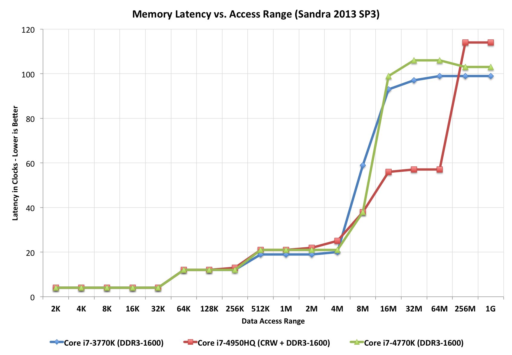
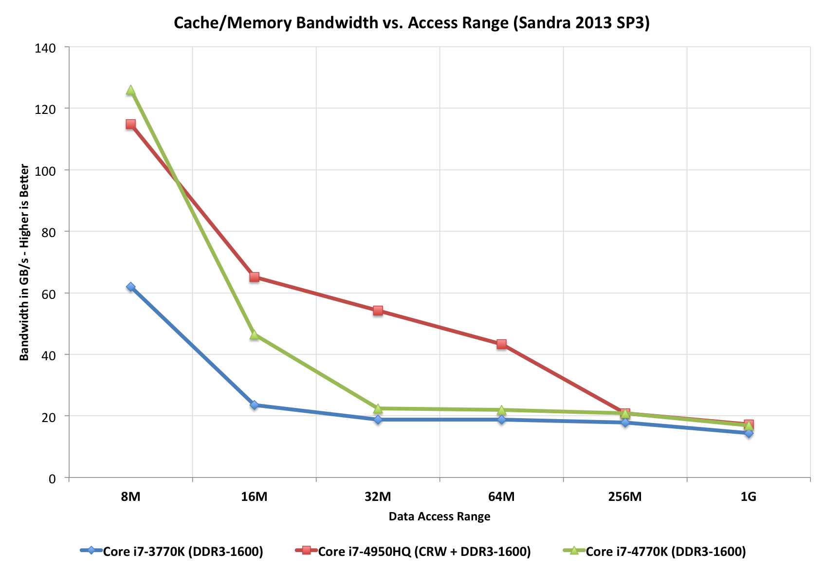
Intel isn’t providing much detail on the connection to Crystalwell other than to say that it’s a narrow, double-pumped serial interface capable of delivering 50GB/s bi-directional bandwidth (100GB/s aggregate). Access latency after a miss in the L3 cache is 30 - 32ns, nicely in between an L3 and main memory access.
The eDRAM clock tops out at 1.6GHz.
There’s only a single size of eDRAM offered this generation: 128MB. Since it’s a cache and not a buffer (and a giant one at that), Intel found that hit rate rarely dropped below 95%. It turns out that for current workloads, Intel didn’t see much benefit beyond a 32MB eDRAM however it wanted the design to be future proof. Intel doubled the size to deal with any increases in game complexity, and doubled it again just to be sure. I believe the exact wording Intel’s Tom Piazza used during his explanation of why 128MB was “go big or go home”. It’s very rare that we see Intel be so liberal with die area, which makes me think this 128MB design is going to stick around for a while.
The 32MB number is particularly interesting because it’s the same number Microsoft arrived at for the embedded SRAM on the Xbox One silicon. If you felt that I was hinting heavily at the Xbox One being ok if its eSRAM was indeed a cache, this is why. I’d also like to point out the difference in future proofing between the two designs.
The Crystalwell enabled graphics driver can choose to keep certain things out of the eDRAM. The frame buffer isn’t stored in eDRAM for example.
| Peak Theoretical Memory Bandwidth | ||||||||||||||||
| Memory Interface | Memory Frequency | Peak Theoretical Bandwidth | ||||||||||||||
| Intel Iris Pro 5200 | 128-bit DDR3 + eDRAM | 1600MHz + 1600MHz eDRAM | 25.6GB/s + 50GB/s eDRAM (bidirectional) | |||||||||||||
| NVIDIA GeForce GT 650M | 128-bit GDDR5 | 5016MHz | 80.3 GB/s | |||||||||||||
| Intel HD 5100/4600/4000 | 128-bit DDR3 | 1600MHz | 25.6GB/s | |||||||||||||
| Apple A6X | 128-bit LPDDR2 | 1066MHz | 17.1 GB/s | |||||||||||||
Intel claims that it would take a 100 - 130GB/s GDDR memory interface to deliver similar effective performance to Crystalwell since the latter is a cache. Accessing the same data (e.g. texture reads) over and over again is greatly benefitted by having a large L4 cache on package.
I get the impression that the plan might be to keep the eDRAM on a n-1 process going forward. When Intel moves to 14nm with Broadwell, it’s entirely possible that Crystalwell will remain at 22nm. Doing so would help Intel put older fabs to use, especially if there’s no need for a near term increase in eDRAM size. I asked about the potential to integrate eDRAM on-die, but was told that it’s far too early for that discussion. Given the size of the 128MB eDRAM on 22nm (~84mm^2), I can understand why. Intel did float an interesting idea by me though. In the future it could integrate 16 - 32MB of eDRAM on-die for specific use cases (e.g. storing the frame buffer).
Intel settled on eDRAM because of its high bandwidth and low power characteristics. According to Intel, Crystalwell’s bandwidth curve is very flat - far more workload independent than GDDR5. The power consumption also sounds very good. At idle, simply refreshing whatever data is stored within, the Crystalwell die will consume between 0.5W and 1W. Under load, operating at full bandwidth, the power usage is 3.5 - 4.5W. The idle figures might sound a bit high, but do keep in mind that since Crystalwell caches both CPU and GPU memory it’s entirely possible to shut off the main memory controller and operate completely on-package depending on the workload. At the same time, I suspect there’s room for future power improvements especially as Crystalwell (or a lower power derivative) heads towards ultra mobile silicon.
Crystalwell is tracked by Haswell’s PCU (Power Control Unit) just like the CPU cores, GPU, L3 cache, etc... Paying attention to thermals, workload and even eDRAM hit rate, the PCU can shift power budget between the CPU, GPU and eDRAM.
Crystalwell is only offered alongside quad-core GT3 Haswell. Unlike previous generations of Intel graphics, high-end socketed desktop parts do not get Crystalwell. Only mobile H-SKUs and desktop (BGA-only) R-SKUs have Crystalwell at this point. Given the potential use as a very large CPU cache, it’s a bit insane that Intel won’t even offer a single K-series SKU with Crystalwell on-board.
As for why lower end parts don’t get it, they simply don’t have high enough memory bandwidth demands - particularly in GT1/GT2 graphics configurations. According to Intel, once you get to about 18W then GT3e starts to make sense but you run into die size constraints there. An Ultrabook SKU with Crystalwell would make a ton of sense, but given where Ultrabooks are headed (price-wise) I’m not sure Intel could get any takers.


177 Comments
View All Comments
8steve8 - Saturday, June 1, 2013 - link
Great work intel, and great review anand.As a fan of low power and small form factor high performance pcs, I'm excited about the 4770R.
my question is how do we get a system with 4770R ?
will it be in an NUC, if so, when/info?
will there be mini-itx motherboards with it soldered on?
bill5 - Saturday, June 1, 2013 - link
Anand, would you say the lack of major performance improvement due to crystalwell bodes ill for Xbox one?The idea is ESRAM could make the 1.2 TF Xbox One GPU "punch above it's weight" with more efficiency due to the 32MB of low latency cache (ALU's will stall less waiting on data). However these results dont really show that for Haswell (the compute results that scale perfectly with ALU's for example).
Here note I'm distinguishing between the cache as bandwidth saver, I think we can all agree it will serve that purpose- and as actual performance enhancer. I'm interested in the latter for Xbox One.
Kevin G - Saturday, June 1, 2013 - link
A couple of quotes and comments from the article:"If Crystalwell demand is lower than expected, Intel still has a lot of quad-core GT3 Haswell die that it can sell and vice versa."
Intel is handicapping demand for GT3e parts by not shipping them in socketed form. I'd love to upgrade my i7-2600k system to a 4770K+GT3e+TSX setup. Seriously Intel, ship that part and take my money.
"The Crystalwell enabled graphics driver can choose to keep certain things out of the eDRAM. The frame buffer isn’t stored in eDRAM for example."
WTF?!? The eDRAM would be the ideal place to store various frequently used buffers. Having 128 MB of memory leaves plenty of room for streaming in textures as need be. The only reason not to hold the full frame buffer is if Intel has an aggressive tile based rendering design and only a tile is stored there. I suspect that Intel's driver team will change this in the future.
"An Ultrabook SKU with Crystalwell would make a ton of sense, but given where Ultrabooks are headed (price-wise) I’m not sure Intel could get any takers."
I bet Apple would ship a GT3e based part in the MacBook Air form factor. They'd do something like lower the GPU clocks to prevent it from melting but they want it. It wouldn't surprise me if Apple managed to negotiate a custom part from Intel again.
Ultimatley I'm pleased with GT3e. On the desktop I can see the GPU being used for OpenCL tasks like physics while my Radeon 7970 handles the rest of the graphics load. Or for anything else, I'd like GT3e for the massive L4 cache.
tipoo - Saturday, June 1, 2013 - link
"Ultimatley I'm pleased with GT3e. On the desktop I can see the GPU being used for OpenCL tasks like physics while my Radeon 7970 handles the rest of the graphics load. Or for anything else, I'd like GT3e for the massive L4 cache."I'd love that to work, but what developer would include that functionality for that niche setup?
Kevin G - Saturday, June 1, 2013 - link
OpenCL is supposed to be flexible enough that you can mix execution targets. This also includes the possibility of OpenCL drivers for CPU's in addition to those that use GPU's. At the very least, it'd be nice for a game or application to manually select the OpenCL target in some config file.Egg - Saturday, June 1, 2013 - link
I'm only a noob high school junior, but aren't frame buffers tossed after display? What would be the point of storing a frame buffer? You don't reuse the data in it at all. As far as I know, frame buffer != unpacked textures.Also, aren't most modern fully programmable GPUs not tile based at all?
Also, wasn't it mentioned that K-series parts don't have TSX?
Kevin G - Saturday, June 1, 2013 - link
The z-buffer in particular is written and often read. Deferred rendering also blends multiple buffers together and at 128 MB in size, a deferred render can keep several in that memory. AA algorithms also perform read/writes on the buffer. At some point, I do see Intel moving the various buffers into the 128 MB of eDRAM as drivers mature. In fairness, this change may not be universal to all games and dependent on things like resolution.Then again, it could be a true cache for the GPU. This would mean that the drivers do not explicitly store the frame buffers there but can could be stored there based upon prefetching of data. Intel's caching hierarchy is a bit weird as the CPU's L3 cache can also be used as a L4 cache for the GPU under HD2000/2500/3000/4000 parts. Presumably the eDRAM would be a L5 cache under the Sandy Bridge/Ivy Bridge schema. The eDRAM has been described as a victim cache though for GPU operations it would make sense to prefetch large amounts of data (textures, buffers). It'd be nice to get some clarification on this with Haswell.
PowerVR is still tile based. Previous Intel integrated solutions were also tile base though they dropped that with the HD line (and I can't remember if the GMA line was tile based as well).
And you are correct that the K series don't have TSX, hence why I'd like a 4770K with GT3e and TSX. Also I forgot to throw in VT-d since that too is arbitrarily disabled in the K series.
IntelUser2000 - Sunday, June 2, 2013 - link
Kevin G: Intel dropped the Tile-based rendering in the GMA 3 series generation back in 2006. Although, their Tile rendering was different from PowerVR's.Egg - Sunday, June 2, 2013 - link
Fair points - I was being a bit myopic and only thought about buffers persisting across frames, neglecting the fact that buffers often need to be reused within the process of rendering a single frame! Can you explain how the CPU's L3 cache is an L4 cache for the GPU? Does the GPU have its own L3 cache already?Also I don't know whether PowerVR's architecture is considered fully programmable yet. I know they have OpenCL capabilities, but reading http://www.anandtech.com/show/6112/qualcomms-quadc... I'm getting a vague feeling that it isn't as complete as GCN or Kepler, feature wise.
IntelUser2000 - Tuesday, June 4, 2013 - link
Gen 7, the Ivy Bridge generation, has its own L3 cache. So you have the LLC(which is L3 for the CPU), and its own L3. Haswell is Gen 7.5.