Intel Iris Pro 5200 Graphics Review: Core i7-4950HQ Tested
by Anand Lal Shimpi on June 1, 2013 10:01 AM ESTHaswell GPU Architecture & Iris Pro
In 2010, Intel’s Clarkdale and Arrandale CPUs dropped the GMA (Graphics Media Accelerator) label from its integrated graphics. From that point on, all Intel graphics would be known as Intel HD graphics. With certain versions of Haswell, Intel once again parts ways with its old brand and introduces a new one, this time the change is much more significant.
Intel attempted to simplify the naming confusion with this slide:
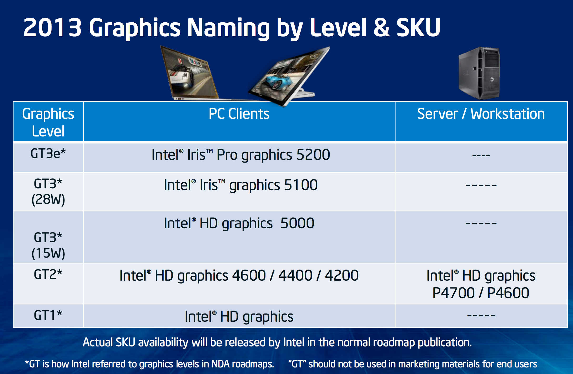
While Sandy and Ivy Bridge featured two different GPU implementations (GT1 and GT2), Haswell adds a third (GT3).
Basically it boils down to this. Haswell GT1 is just called Intel HD Graphics, Haswell GT2 is HD 4200/4400/4600. Haswell GT3 at or below 1.1GHz is called HD 5000. Haswell GT3 capable of hitting 1.3GHz is called Iris 5100, and finally Haswell GT3e (GT3 + embedded DRAM) is called Iris Pro 5200.
The fundamental GPU architecture hasn’t changed much between Ivy Bridge and Haswell. There are some enhancements, but for the most part what we’re looking at here is a dramatic increase in the amount of die area allocated for graphics.
All GPU vendors have some fundamental building block they scale up/down to hit various performance/power/price targets. AMD calls theirs a Compute Unit, NVIDIA’s is known as an SMX, and Intel’s is called a sub-slice.
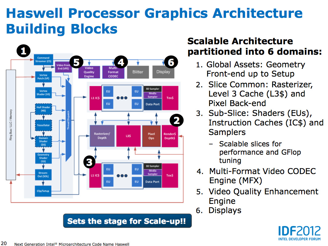
In Haswell, each graphics sub-slice features 10 EUs. Each EU is a dual-issue SIMD machine with two 4-wide vector ALUs:
| Low Level Architecture Comparison | ||||||||||||||||
| AMD GCN | Intel Gen7 Graphics | NVIDIA Kepler | ||||||||||||||
| Building Block | GCN Compute Unit | Sub-Slice | Kepler SMX | |||||||||||||
| Shader Building Block | 16-wide Vector SIMD | 2 x 4-wide Vector SIMD | 32-wide Vector SIMD | |||||||||||||
| Smallest Implementation | 4 SIMDs | 10 SIMDs | 6 SIMDs | |||||||||||||
| Smallest Implementation (ALUs) | 64 | 80 | 192 | |||||||||||||
There are limitations as to what can be co-issued down each EU’s pair of pipes. Intel addressed many of the co-issue limitations last generation with Ivy Bridge, but there are still some that remain.
Architecturally, this makes Intel’s Gen7 graphics core a bit odd compared to AMD’s GCN and NVIDIA’s Kepler, both of which feature much wider SIMD arrays without any co-issue requirements. The smallest sub-slice in Haswell however delivers a competitive number of ALUs to AMD and NVIDIA implementations.
Intel had a decent building block with Ivy Bridge, but it chose not to scale it up as far as it would go. With Haswell that changes. In its highest performing configuration, Haswell implements four sub-slices or 40 EUs. Doing the math reveals a very competent looking part on paper:
| Peak Theoretical GPU Performance | ||||||||||||||||
| Cores/EUs | Peak FP ops per Core/EU | Max GPU Frequency | Peak GFLOPs | |||||||||||||
| Intel Iris Pro 5100/5200 | 40 | 16 | 1300MHz | 832 GFLOPS | ||||||||||||
| Intel HD Graphics 5000 | 40 | 16 | 1100MHz | 704 GFLOPS | ||||||||||||
| NVIDIA GeForce GT 650M | 384 | 2 | 900MHz | 691.2 GFLOPS | ||||||||||||
| Intel HD Graphics 4600 | 20 | 16 | 1350MHz | 432 GFLOPS | ||||||||||||
| Intel HD Graphics 4000 | 16 | 16 | 1150MHz | 294.4 GFLOPS | ||||||||||||
| Intel HD Graphics 3000 | 12 | 12 | 1350MHz | 194.4 GFLOPS | ||||||||||||
| Intel HD Graphics 2000 | 6 | 12 | 1350MHz | 97.2 GFLOPS | ||||||||||||
| Apple A6X | 32 | 8 | 300MHz | 76.8 GFLOPS | ||||||||||||
In its highest end configuration, Iris has more raw compute power than a GeForce GT 650M - and even more than a GeForce GT 750M. Now we’re comparing across architectures here so this won’t necessarily translate into a performance advantage in games, but the takeaway is that with HD 5000, Iris 5100 and Iris Pro 5200 Intel is finally walking the walk of a GPU company.
Peak theoretical performance falls off steeply as soon as you start looking at the GT2 and GT1 implementations. With 1/4 - 1/2 of the execution resources as the GT3 graphics implementation, and no corresponding increase in frequency to offset the loss the slower parts are substantially less capable. The good news is that Haswell GT2 (HD 4600) is at least more capable than Ivy Bridge GT2 (HD 4000).
Taking a step back and looking at the rest of the theoretical numbers gives us a more well rounded look at Intel’s graphics architectures :
| Peak Theoretical GPU Performance | ||||||||||||||||
| Peak Pixel Fill Rate | Peak Texel Rate | Peak Polygon Rate | Peak GFLOPs | |||||||||||||
| Intel Iris Pro 5100/5200 | 10.4 GPixels/s | 20.8 GTexels/s | 650 MPolys/s | 832 GFLOPS | ||||||||||||
| Intel HD Graphics 5000 | 8.8 GPixels/s | 17.6 GTexels/s | 550 MPolys/s | 704 GFLOPS | ||||||||||||
| NVIDIA GeForce GT 650M | 14.4 GPixels/s | 28.8 GTexels/s | 900 MPolys/s | 691.2 GFLOPS | ||||||||||||
| Intel HD Graphics 4600 | 5.4 GPixels/s | 10.8 GTexels/s | 675 MPolys/s | 432 GFLOPS | ||||||||||||
| AMD Radeon HD 7660D (Desktop Trinity, A10-5800K) | 6.4 GPixels/s | 19.2 GTexels/s | 800 MPolys/s | 614 GFLOPS | ||||||||||||
| AMD Radeon HD 7660G (Mobile Trinity, A10-4600M) | 3.97 GPixels/s | 11.9 GTexels/s | 496 MPolys/s | 380 GFLOPS | ||||||||||||
Intel may have more raw compute, but NVIDIA invested more everywhere else in the pipeline. Triangle, texturing and pixel throughput capabilities are all higher on the 650M than on Iris Pro 5200. Compared to AMD's Trinity however, Intel has a big advantage.


177 Comments
View All Comments
8steve8 - Saturday, June 1, 2013 - link
Great work intel, and great review anand.As a fan of low power and small form factor high performance pcs, I'm excited about the 4770R.
my question is how do we get a system with 4770R ?
will it be in an NUC, if so, when/info?
will there be mini-itx motherboards with it soldered on?
bill5 - Saturday, June 1, 2013 - link
Anand, would you say the lack of major performance improvement due to crystalwell bodes ill for Xbox one?The idea is ESRAM could make the 1.2 TF Xbox One GPU "punch above it's weight" with more efficiency due to the 32MB of low latency cache (ALU's will stall less waiting on data). However these results dont really show that for Haswell (the compute results that scale perfectly with ALU's for example).
Here note I'm distinguishing between the cache as bandwidth saver, I think we can all agree it will serve that purpose- and as actual performance enhancer. I'm interested in the latter for Xbox One.
Kevin G - Saturday, June 1, 2013 - link
A couple of quotes and comments from the article:"If Crystalwell demand is lower than expected, Intel still has a lot of quad-core GT3 Haswell die that it can sell and vice versa."
Intel is handicapping demand for GT3e parts by not shipping them in socketed form. I'd love to upgrade my i7-2600k system to a 4770K+GT3e+TSX setup. Seriously Intel, ship that part and take my money.
"The Crystalwell enabled graphics driver can choose to keep certain things out of the eDRAM. The frame buffer isn’t stored in eDRAM for example."
WTF?!? The eDRAM would be the ideal place to store various frequently used buffers. Having 128 MB of memory leaves plenty of room for streaming in textures as need be. The only reason not to hold the full frame buffer is if Intel has an aggressive tile based rendering design and only a tile is stored there. I suspect that Intel's driver team will change this in the future.
"An Ultrabook SKU with Crystalwell would make a ton of sense, but given where Ultrabooks are headed (price-wise) I’m not sure Intel could get any takers."
I bet Apple would ship a GT3e based part in the MacBook Air form factor. They'd do something like lower the GPU clocks to prevent it from melting but they want it. It wouldn't surprise me if Apple managed to negotiate a custom part from Intel again.
Ultimatley I'm pleased with GT3e. On the desktop I can see the GPU being used for OpenCL tasks like physics while my Radeon 7970 handles the rest of the graphics load. Or for anything else, I'd like GT3e for the massive L4 cache.
tipoo - Saturday, June 1, 2013 - link
"Ultimatley I'm pleased with GT3e. On the desktop I can see the GPU being used for OpenCL tasks like physics while my Radeon 7970 handles the rest of the graphics load. Or for anything else, I'd like GT3e for the massive L4 cache."I'd love that to work, but what developer would include that functionality for that niche setup?
Kevin G - Saturday, June 1, 2013 - link
OpenCL is supposed to be flexible enough that you can mix execution targets. This also includes the possibility of OpenCL drivers for CPU's in addition to those that use GPU's. At the very least, it'd be nice for a game or application to manually select the OpenCL target in some config file.Egg - Saturday, June 1, 2013 - link
I'm only a noob high school junior, but aren't frame buffers tossed after display? What would be the point of storing a frame buffer? You don't reuse the data in it at all. As far as I know, frame buffer != unpacked textures.Also, aren't most modern fully programmable GPUs not tile based at all?
Also, wasn't it mentioned that K-series parts don't have TSX?
Kevin G - Saturday, June 1, 2013 - link
The z-buffer in particular is written and often read. Deferred rendering also blends multiple buffers together and at 128 MB in size, a deferred render can keep several in that memory. AA algorithms also perform read/writes on the buffer. At some point, I do see Intel moving the various buffers into the 128 MB of eDRAM as drivers mature. In fairness, this change may not be universal to all games and dependent on things like resolution.Then again, it could be a true cache for the GPU. This would mean that the drivers do not explicitly store the frame buffers there but can could be stored there based upon prefetching of data. Intel's caching hierarchy is a bit weird as the CPU's L3 cache can also be used as a L4 cache for the GPU under HD2000/2500/3000/4000 parts. Presumably the eDRAM would be a L5 cache under the Sandy Bridge/Ivy Bridge schema. The eDRAM has been described as a victim cache though for GPU operations it would make sense to prefetch large amounts of data (textures, buffers). It'd be nice to get some clarification on this with Haswell.
PowerVR is still tile based. Previous Intel integrated solutions were also tile base though they dropped that with the HD line (and I can't remember if the GMA line was tile based as well).
And you are correct that the K series don't have TSX, hence why I'd like a 4770K with GT3e and TSX. Also I forgot to throw in VT-d since that too is arbitrarily disabled in the K series.
IntelUser2000 - Sunday, June 2, 2013 - link
Kevin G: Intel dropped the Tile-based rendering in the GMA 3 series generation back in 2006. Although, their Tile rendering was different from PowerVR's.Egg - Sunday, June 2, 2013 - link
Fair points - I was being a bit myopic and only thought about buffers persisting across frames, neglecting the fact that buffers often need to be reused within the process of rendering a single frame! Can you explain how the CPU's L3 cache is an L4 cache for the GPU? Does the GPU have its own L3 cache already?Also I don't know whether PowerVR's architecture is considered fully programmable yet. I know they have OpenCL capabilities, but reading http://www.anandtech.com/show/6112/qualcomms-quadc... I'm getting a vague feeling that it isn't as complete as GCN or Kepler, feature wise.
IntelUser2000 - Tuesday, June 4, 2013 - link
Gen 7, the Ivy Bridge generation, has its own L3 cache. So you have the LLC(which is L3 for the CPU), and its own L3. Haswell is Gen 7.5.