AMD’s Jaguar Architecture: The CPU Powering Xbox One, PlayStation 4, Kabini & Temash
by Anand Lal Shimpi on May 23, 2013 12:00 AM EST
Microprocessor architectures these days are largely limited, and thus defined, by power consumption. When it comes to designing an architecture around a power envelope the rule of thumb is any given microprocessor architecture can scale to target an order of magnitude of TDPs. For example, Intel’s Core architectures (Sandy/Ivy Bridge) effectively target the 13W - 130W range. They can surely be used in parts that consume less or more power, but at those extremes it’s more efficient to build another microarchitecture to target those TDPs instead.
Both AMD and Intel feel similarly about this order of magnitude rule, and thus both have two independent microprocessor architectures that they leverage to build chips for the computing continuum. From Intel we have Atom for low power, and Core for high performance. In 2010 AMD gave us Bobcat for its low power roadmap, and Bulldozer for high performance.
Both the Bobcat and Bulldozer lines would see annual updates. In 2011 we saw Bobcat used in Ontario and Zacate SoCs, as a part of the Brazos platform. Last year AMD announced Brazos 2.0, using slightly updated versions of those very same Bobcat based SoCs. Today AMD officially launches Kabini and Temash, APUs based on the first major architectural update to Bobcat: the Jaguar core.


Jaguar: Improved 2-wide Out-of-Order
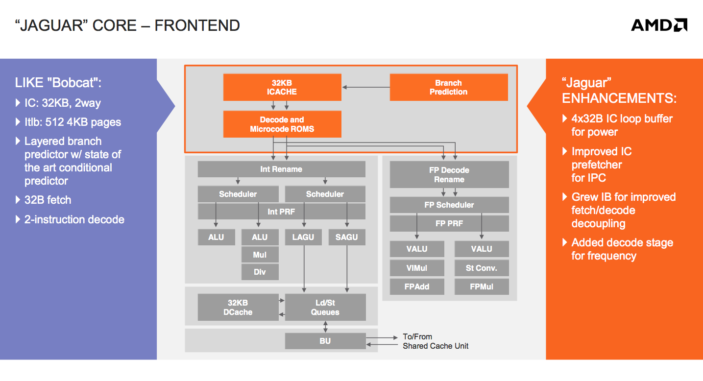
At the core-level, Jaguar still looks a lot like Bobcat. The same dual-issue, out-of-order architecture that AMD introduced in 2010 remains intact with Jaguar. The same L1 cache, front end and execution blocks are all still here. Given the ARM transition from a dual-issue, out-of-order core with Cortex A9 to a three-issue, OoO design with the Cortex A15, I expected something similar from AMD. Despite moving to a smaller manufacturing process (28nm), AMD was very focused on increasing performance within the same TDP or lower with Jaguar. The driving motivator? While Bobcat ended up in netbooks, nettops and other low cost, but thick machines, Jaguar needed to go into even thinner form factors: tablets. AMD still has no intentions of getting into the smartphone SoC space, but the Windows 8 (and Android?) tablet market is fair game. Cellular connectivity isn’t a requirement there, particularly at the lower price points, and AMD can easily be a second source alternative to Intel Atom based designs.
The average number of instructions executed per clock (IPC) is still below 1 for most client workloads. There’s a certain amount of burst traffic to be expected but given the types of dependencies you see in most use cases, AMD felt the gain from making the machine wider wasn’t worth the power tradeoff. There’s also the danger of making the cat-cores too powerful. While just making them 3-issue to begin with wouldn’t dramatically close the gap between the cat-cores and the Bulldozer family, there’s still a desire for there to be clear separation between the two microarchitectures.
The move to a three-issue design would certainly increase performance, but AMD’s tablet ambitions and power sensitivity meant it would save that transition for another day. I should point out that ARM is increasingly looking like the odd-man-out here, with both Jaguar and Intel’s Silvermont retaining the dual-issue design of their predecessors. Part of this has to do with the fact that while AMD and Intel are very focused on driving power down, ARM has aspirations of moving up in the performance/power chain.
The width of the front end is only one lever AMD could have used to increase performance. While it was a pretty big lever that AMD chose not to pull, there are other smaller levers that were exercised in Jaguar.
There’s now a 4 x 32-byte loop buffer for the instruction cache. Whenever a loop is detected, instead of fetching instructions executed in the loop from the L1 I-cache over and over again, they’re serviced from this small loop buffer. If this sounds like a trace cache or decoded micro-op cache, don’t get too excited, Jaguar’s loop buffer is neither of these things. There are no pipeline savings or powered down fetch/decode units. The only benefit to the new loop buffer is the instruction cache doesn’t have to be fired up during every iteration of a buffered loop. In other words, this is a very specific play to reduce power consumption - not to improve performance.
All microprocessors see tons of simulation work before they’re ever brought to market. Even once a design is done, additional profiling is used to identify bottlenecks, which are then prioritized for addressing in future designs. All bottleneck removal has to be vetted against power, cost and schedule constraints. Given an infinite budget across all vectors you could eliminate all bottlenecks, but you’d likely take an infinite amount of time to complete the design. Taking all of those realities into account usually means making tradeoffs, even when improving a design.
We saw the first example of a clear tradeoff when AMD stuck with a 2-issue front end for Jaguar. Not including a decoded micro-op cache and opting for a simpler loop buffer instead is an example of another. AMD likely noticed a lot of power being wasted during loops, and the addition of a loop buffer was probably the best balance of complexity, power savings and cost.
AMD also improved the instruction cache prefetcher, not because of an over abundance of bandwidth but by revisiting the Bobcat design and spending some more time on the implementation in Jaguar. The IC prefetcher improvements are simply AMD doing things better in Jaguar, not being under the same pressure to introduce a brand new architecture as was the case with Bobcat.
The instruction buffer between the instruction cache and decoders grew in size with Jaguar, a sort of half step towards the more heavily decoupled fetch/decode stages in Bulldozer.
Jaguar adds support for new instructions (SSE4.1/4.2, AES, CLMUL, MOVBE, AVX, F16C, BMI1) as well as 40-bit physical addressing.
The final change to the front of Jaguar was the addition of another decode stage, purely for frequency gains. It turns out that in Bobcat the decoder was one of the critical paths limiting maximum frequency. Adding another decode stage simply gave AMD enough wiggle room to hit their frequency targets for Jaguar at 28nm.


78 Comments
View All Comments
skatendo - Friday, May 24, 2013 - link
Not entirely true. The Wii U CPU is highly customized and has enhancements not found in typical PowerPC processors. It's been completely tailored for gaming. I'm not saying it's the power of the newer Jaguar chipsets, but the beauty of custom silicon is that you can do much more with less (Tegra 3's quad-core, 12-core GPU vs. Apple's A5 dual core CPU/GPU anyone? yeah A5 kicked its arse for games) that's why Nintendo didn't release tech specs because they tailored a system for games and performance will manifest with upcoming games (not these sloppy ports we've seen so far).tipoo - Friday, May 24, 2013 - link
I'm aware it would be highly customized, but a plethora of developers have also come out and said the CPU sucks.skatendo - Saturday, May 25, 2013 - link
Also the "plethora" of developers that said it sucked (namely the Metro: Last Light dev) said they had an early build of the Wii U SDK and said it was "slow". Having worked for a developer, they base their opinions on how fast/efficient they can port over their game. The Wii U is a totally different infrastructure that lazy devs don't want to take the time to learn, especially with a newer GPGPU.Kevin G - Sunday, May 26, 2013 - link
If a developer wants to do GPGPU, the PS4 and Xbox One will be highly preferable due to unified virtual memory space. If GPGPU was Nintendo's strategy, they shouldn't have picked a GPU from the Radeon 6000 generation. Sure, it can do GPU but there are far more compromises to hand off the workload.Simen1 - Thursday, May 23, 2013 - link
What is the TDP and die size of the APUs in X-Box One and Playstation 4?haukionkannel - Thursday, May 23, 2013 - link
Douple the 1.6 Ghz 4 core version and you are near. The wider memory controller eats some extra energy to, so maybe you have to add 0.2 to 0.3 calculation...fellix - Thursday, May 23, 2013 - link
"The L2 cache is also inclusive, a first in AMD’s history."Not exactly correct. The very first Athon (K7) on Slot A with off-die L2 used inclusive cache hierarchy. All models after that moved to exclusive design.
Exophase - Thursday, May 23, 2013 - link
Bulldozer is also mostly inclusive. Not strictly inclusive, but certainly not exclusive (you really wouldn't get such a thing from a writethrough L1 cache)whyso - Thursday, May 23, 2013 - link
Ahh amd, I love your marketing slides. Lets compare battery life and EXCLUDE the screen. Never mind that the screen consumes a large amount of power and that when you add it to the total battery life savings go down tremendously. (That's why sandy-> ivy bridge didn't improve battery life that much on mobile). Lets also leave out the Rest of system power and soc power for brazos. It also looks like the system is using an SSD to generate these numbers which looking at the target market almost no OEM will do.extide - Thursday, May 23, 2013 - link
It's a perfectly valid comparison to make. All laptops will include a screen and the screen has nothing to do with AMD (or Intel).