The Xbox One: Hardware Analysis & Comparison to PlayStation 4
by Anand Lal Shimpi on May 22, 2013 8:00 AM ESTCPU & GPU Hardware Analyzed
Although Microsoft did its best to minimize AMD’s role in all of this, the Xbox One features a semi-custom 28nm APU designed with AMD. If this sounds familiar it’s because the strategy is very similar to what Sony employed for the PS4’s silicon.
The phrase semi-custom comes from the fact that AMD is leveraging much of its already developed IP for the SoC. On the CPU front we have two Jaguar compute units, each one with four independent processor cores and a shared 2MB L2 cache. The combination of the two give the Xbox One its 8-core CPU. This is the same basic layout of the PS4‘s SoC.
If you’re not familiar with it, Jaguar is the follow-on to AMD’s Bobcat core - think of it as AMD’s answer to the Intel Atom. Jaguar is a 2-issue OoO architecture, but with roughly 20% higher IPC than Bobcat thanks to a number of tweaks. In ARM terms we’re talking about something that’s faster than a Cortex A15. I expect Jaguar to be close but likely fall behind Intel’s Silvermont, at least at the highest shipping frequencies. Jaguar is the foundation of AMD’s Kabini and Temash APUs, where it will ship first. I’ll have a deeper architectural look at Jaguar later this week. Update: It's live!
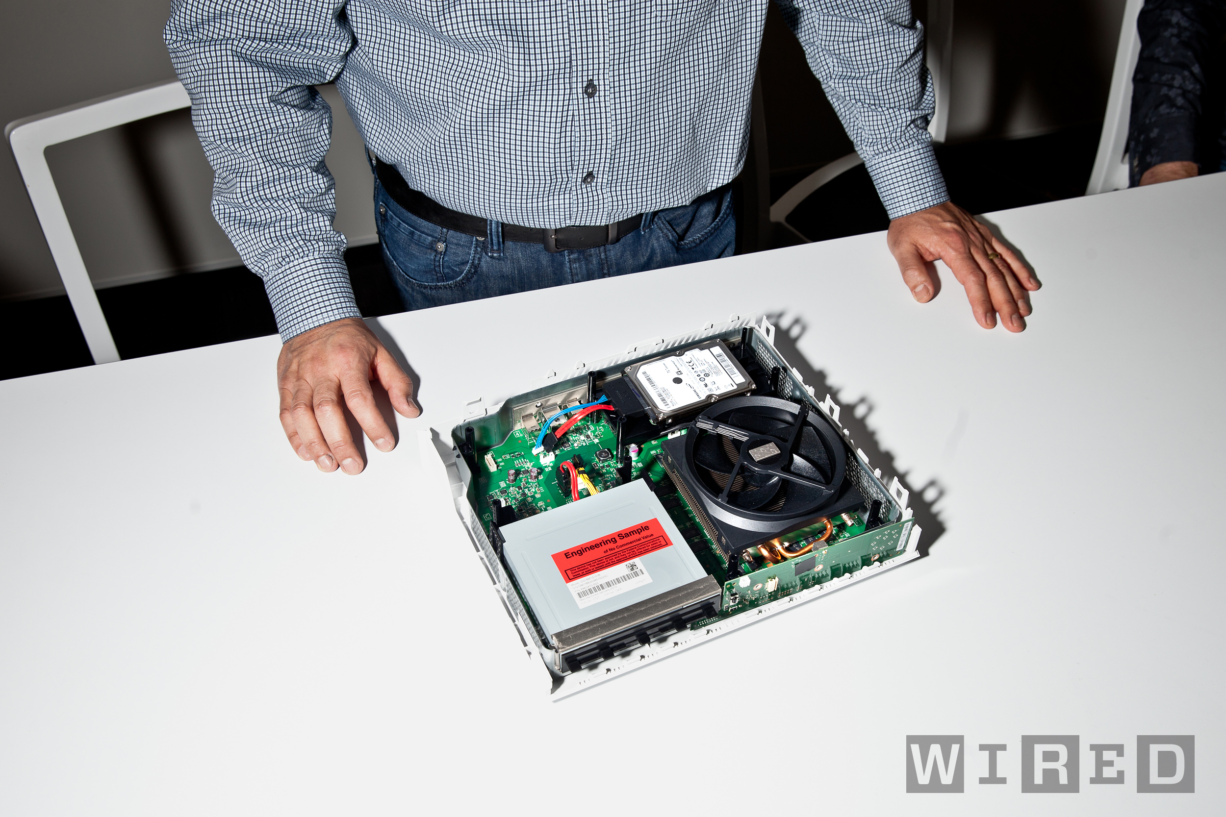 Inside the Xbox One, courtesy Wired
There’s no word on clock speed, but Jaguar at 28nm is good for up to 2GHz depending on thermal headroom. Current rumors point to both the PS4 and Xbox One running their Jaguar cores at 1.6GHz, which sounds about right. In terms of TDP, on the CPU side you’re likely looking at 30W with all cores fully loaded.
The move away from PowerPC to 64-bit x86 cores means the One breaks backwards compatibility with all Xbox 360 titles. Microsoft won’t be pursuing any sort of a backwards compatibility strategy, although if a game developer wanted to it could port an older title to the new console. Interestingly enough, the first Xbox was also an x86 design - from a hardware/ISA standpoint the new Xbox One is backwards compatible with its grandfather, although Microsoft would have to enable that as a feature in software - something that’s quite unlikely.
| Microsoft Xbox One vs. Sony PlayStation 4 Spec comparison | ||||||||||||||
| Xbox 360 | Xbox One | PlayStation 4 | ||||||||||||
| CPU Cores/Threads | 3/6 | 8/8 | 8/8 | |||||||||||
| CPU Frequency | 3.2GHz | 1.6GHz (est) | 1.6GHz (est) | |||||||||||
| CPU µArch | IBM PowerPC | AMD Jaguar | AMD Jaguar | |||||||||||
| Shared L2 Cache | 1MB | 2 x 2MB | 2 x 2MB | |||||||||||
| GPU Cores | 768 | 1152 | ||||||||||||
| Peak Shader Throughput | 0.24 TFLOPS | 1.23 TFLOPS | 1.84 TFLOPS | |||||||||||
| Embedded Memory | 10MB eDRAM | 32MB eSRAM | - | |||||||||||
| Embedded Memory Bandwidth | 32GB/s | 102GB/s | - | |||||||||||
| System Memory | 512MB 1400MHz GDDR3 | 8GB 2133MHz DDR3 | 8GB 5500MHz GDDR5 | |||||||||||
| System Memory Bus | 128-bits | 256-bits | 256-bits | |||||||||||
| System Memory Bandwidth | 22.4 GB/s | 68.3 GB/s | 176.0 GB/s | |||||||||||
| Manufacturing Process | 28nm | 28nm | ||||||||||||
On the graphics side it’s once again obvious that Microsoft and Sony are shopping at the same store as the Xbox One’s SoC integrates an AMD GCN based GPU. Here’s where things start to get a bit controversial. Sony opted for an 18 Compute Unit GCN configuration, totaling 1152 shader processors/cores/ALUs. Microsoft went for a far smaller configuration: 768 (12 CUs).
Microsoft can’t make up the difference in clock speed alone (AMD’s GCN seems to top out around 1GHz on 28nm), and based on current leaks it looks like both MS and Sony are running their GPUs at the same 800MHz clock. The result is a 33% reduction in compute power, from 1.84 TFLOPs in the PS4 to 1.23 TFLOPs in the Xbox One. We’re still talking about over 5x the peak theoretical shader performance of the Xbox 360, likely even more given increases in efficiency thanks to AMD’s scalar GCN architecture (MS quotes up to 8x better GPU performance) - but there’s no escaping the fact that Microsoft has given the Xbox One less GPU hardware than Sony gave the PlayStation 4. Note that unlike the Xbox 360 vs. PS3 era, Sony's hardware advantage here won't need any clever developer work to extract - the architectures are near identical, Sony just has more resources available to use.
Remember all of my talk earlier about a slight pivot in strategy? Microsoft seems to believe that throwing as much power as possible at the next Xbox wasn’t the key to success and its silicon choices reflect that.


245 Comments
View All Comments
sri_tech - Wednesday, May 22, 2013 - link
Anand,I replied to you on twitter that this is 28nm SoC. You asked for "source".
As usual, good article.
ON A PALE HOR5E - Wednesday, December 18, 2013 - link
Ok, I am going off on a tangent. I understand technology is expanding, and that CPU's have a huge amount of transistors now on a single die. So with our knowledge and manufacturing capabilities, why are we still make motherboards as big as a VCR? Seems to me a lot of space could be save by creating a semiconductor die, for all those capacitor's, resistor's, inductor's, and other semiconductor packages. After all your spending all that money to develop a new system. Why not make it a sportier, Lighter in weight, and tie it with the newest VR gear, and have a gaming anywhere super system?Shadowmaster625 - Wednesday, May 22, 2013 - link
The embedded RAM + DDR3 paradigm is sort of a gimme to Intel. It probably will not even be that long before intel starts shipping a CPU with embedded RAM and their equivalent of 768 AMD shaders (3x HD5200?). When they do they will be able to snatch up a handful of developers with lots of experience working with that exact setup. It seems like a mistake for AMD to provide such a design knowing it is going to hurt them down the road. This is another "what the hell were they thinking" moments.tipoo - Wednesday, May 22, 2013 - link
Intel is already going down the embedded memory route, AMD is not "providing" anything to them here that they wouldn't already make.Gigaplex - Wednesday, May 22, 2013 - link
I think Shadowmaster625 was implying that AMD is giving developers experience working on such a platform ready for Intel to come in and sweep them up. I don't think it's relevant as there's nothing particularly exotic about having a small amount of fast memory when you consider how developers have had to deal with the Cell chip.tipoo - Wednesday, May 22, 2013 - link
Ah, perhaps I misunderstood. But if it's automatically managed (and Haswell at least certainly is) that's not a consideration.80's Kidd - Thursday, May 23, 2013 - link
Embedded memory is nothing new, Intel had it first with the L1 and L2 cache in the early 90's with their Pentium Pro line.Oxford Guy - Wednesday, January 21, 2015 - link
I think the first microprocessor with embedded memory was the 1975 Fairchild F8 which had 64 bytes of scratchpad. The Motorola 68k line also had internal cache before Intel's x86. The 68040 from 1990 had the same amount of internal cache, 8KiB, as the Pentium Pro. The Pentium Pro, though, had a large on package cache (256KiB to 1 MiB).mfenn - Wednesday, May 22, 2013 - link
So AMD should give up a guaranteed revenue stream from the two biggest console manufacturers for 10+ years just so they won't (as a side effect) train developers on an obvious architecture? That doesn't make any sense.kyuu - Wednesday, May 22, 2013 - link
Don't be absurd. One, this is nothing new. The Xbox 360 used embedded eDRAM, and other consoles have before it.Two, AMD is going to start embedding eDRAM into its APUs in the near future as well.