NVIDIA Tegra 4 Architecture Deep Dive, Plus Tegra 4i, Icera i500 & Phoenix Hands On
by Anand Lal Shimpi & Brian Klug on February 24, 2013 3:00 PM ESTEver since NVIDIA arrived on the SoC scene, it has done a great job of introducing its ultra mobile SoCs. Tegra 2 and 3 were both introduced with a healthy amount of detail and the sort of collateral we expect to see from any PC silicon vendor. While the rest of the mobile space is slowly playing catchup, NVIDIA continued the trend with its Tegra 4 and Tegra 4i architecture disclosure.
Since Tegra 4i is a bit further out, much of NVIDIA’s focus for today’s disclosure focused on its flagship Tegra 4 SoC due to begin shipping in Q2 of this year along with the NVIDIA i500 baseband. At a high level you’re looking at a quad-core ARM Cortex A15 (plus fifth A15 companion core) and a 72-core GeForce GPU. To understand Tegra 4 at a lower level, we’ll dive into the individual blocks beginning, as usual with the CPU.
ARM’s Cortex A15 and Power Consumption
Tegra 4’s CPU complex sees a significant improvement over Tegra 3. Despite being an ARM architecture licensee, NVIDIA once again licensed a complete processor from ARM rather than designing its own core. I do fundamentally believe that NVIDIA will go the full custom route eventually (see: Project Denver), but that’s a goal that will take time to come to fruition.
In the case of Tegra 4, NVIDIA chose to license ARM’s Cortex A15 - the only vanilla ARM core presently offered that can deliver higher performance than a Cortex A9.
Samsung recently disclosed details about its Cortex A15 implementation compared to the Cortex A7, a similarly performing but more power efficient alternative to the A9. In its ISSCC paper on the topic Samsung noted that the Cortex A15 offered up to 3x the performance of the Cortex A7, at 4x the area and 6x the power consumption. It’s a tremendous performance advantage for sure, but it comes at a great cost to area and power consumption. The area side isn’t as important as NVIDIA has to eat that cost, but power consumption is a valid concern.
To ease fears about power consumption, NVIDIA provided the following data:
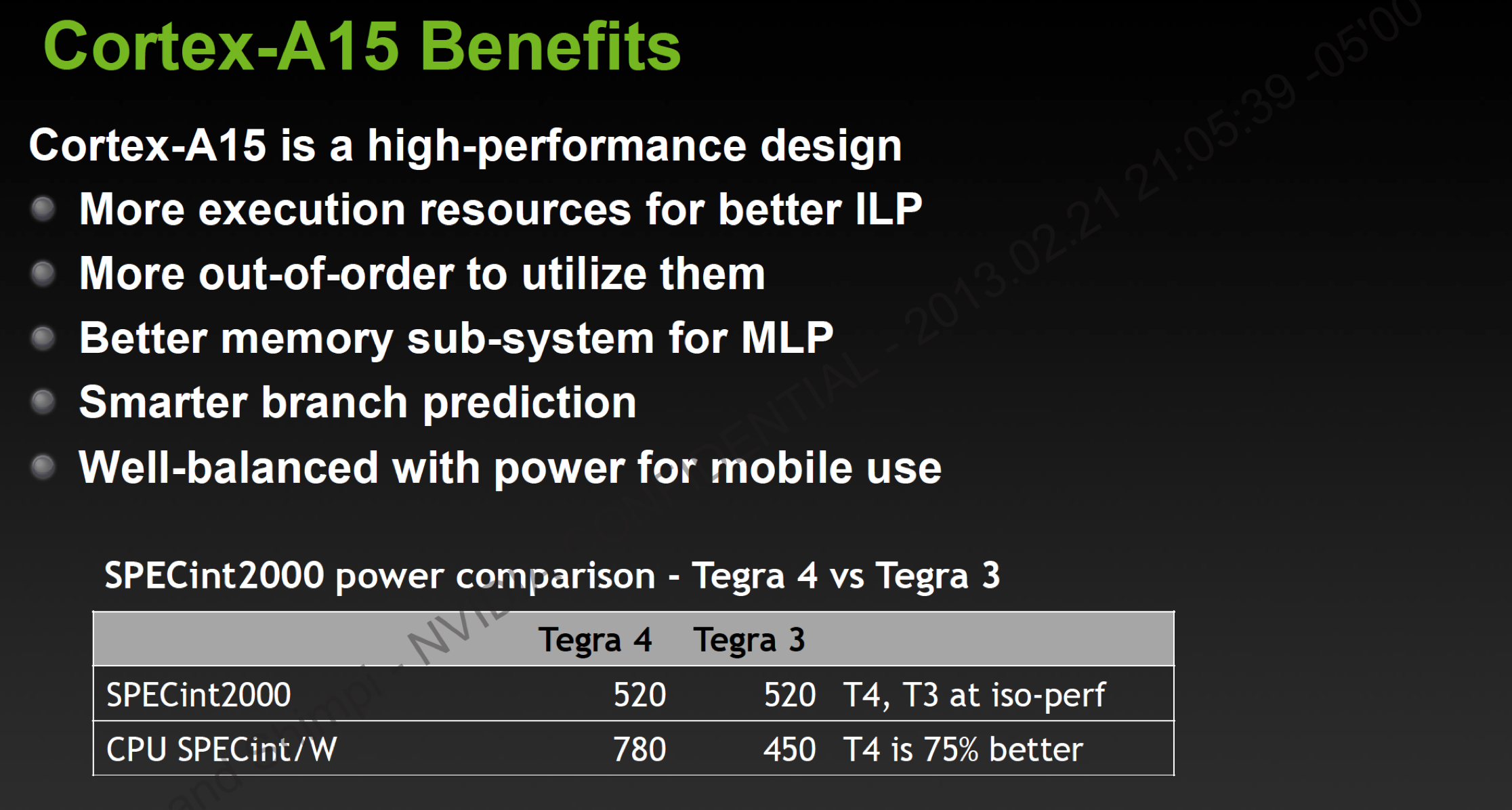
The table above is a bit confusing so let me explain. In the first row NVIDIA is showing that it has configured the Tegra 3 and 4 platforms to deliver the same SPECint_base 2000 performance. SPECint is a well respected CPU benchmark that stresses everything from the CPU core to the memory interface. The int at the end of the name implies that we’re looking at purely single threaded integer performance.
The second row shows us the SPECint per watt of the Tegra 3/4 CPU subsystem, when running at the frequencies required to deliver a SPECint score of 520. By itself this doesn’t tell us a whole lot, but we can use this data to get some actual power numbers.
At the same performance level, Tegra 4 operates at 40% lower power than Tegra 3. The comparison is unfortunately not quite apples to apples as we’re artificially limiting Tegra 4’s peak clock speed, while running Tegra 3 at its highest, most power hungry state. The clocks in question are 1.6GHz for Tegra 3 and 825MHz for Tegra 4. Running at lower clocks allows you to run at a lower voltage, which results in much lower power consumption. In other words, NVIDIA’s comparison is useful but skewed in favor of Tegra 4.
What this data does tell us however is exactly how NVIDIA plans on getting Tegra 4 into a phone: by aggressively limiting frequency. If a Cortex A15 at 825MHz delivers identical performance at a lower power compared to a 40nm Cortex A9 at 1.6GHz, it’s likely possible to deliver a marginal performance boost without breaking the power bank.
That 825MHz mark ends up being an important number, because that’s where the fifth companion Cortex A15 tops out at. I suspect that in a phone configuration NVIDIA might keep everything running on the companion core for as long as possible, which would address my fears about typical power consumption in a phone. Peak power consumption is still going to be a problem I think.


75 Comments
View All Comments
PingviN - Monday, February 25, 2013 - link
Tegra made an operating loss of $150 million for fiscal year 2012, despite getting into both the Nexus 7 (the refresh coming this year has been lost to Qualcomm) and the Surface RT. Sales prognosis cut almost in half for the fiscal year 2013. To date, Nvidia hasn't had any profit coming out of Tegra and now it's in limbo mode until Tegra 4 is released because Tegra 3 gets smashed by it's competition.It's been a pretty crappy year for Tegra.
guilmon14 - Tuesday, February 26, 2013 - link
I don't know anything about this company "tegra", but have you heard about Nvidia? I heard they're doing great!http://nvidianews.nvidia.com/Releases/NVIDIA-Repor...
According to this Nvidia is up in income, revenue, and equity.
If you wanted to check the easy way just look at nvidia's wikipedia page, gives you all the nice money numbers.
http://en.wikipedia.org/wiki/Nvidia
trajan2448 - Monday, February 25, 2013 - link
5 years down the road phones will be cooking our dinner. It's amazing how fast the tech is advancing now.Scannall - Monday, February 25, 2013 - link
If they don't hustle right along, SOC's with the PowerVR 6 series (Rogue) will beat them to market. And considering their GPU just barely squeaks by the iPad as it is, it will be behind early on.Khato - Monday, February 25, 2013 - link
Was it specifically stated that the Tegra 4 SPECint/W figure was running on the high speed cores? As is mentioned later on the page, a SPECint2000 of 520 is within reach of the power optimized companion core, so the only reason I'd expect NVIDIA to not use the companion core for this data is if they explicitly stated that it wasn't.Part of the cause for my suspicion is that the Power vs DMIPS chart that Samsung recently provided for the Exynos 5 Octa shows 8k DMIPS at 1 watt... and from the press coverage back in 2009 for the A9 hard macros there's both the 10k DMIPS at 1.9 watts and 2GHz with the speed speed optimized and 4k DMIPS at 250 mW and 800 MHz for the power optimized. Which equate to 5.26 DMIPS/mW and 8 DMIPS/mW, respectively. Now the 2GHz data point should be even worse off than Tegra 3 and yet it only shows the Samsung Exynos 5 Octa as being 52% more efficient.
Going into estimating rather than published numbers, if we up the efficiency of Tegra 3 a bit compared to that 2GHz figure then it's likely going to be closer to A15 being 30% more efficient... which you then add the known ~40% efficiency bump going from a performance to power implementation and you get the kind of drastic increase NVIDIA is touting.
Wilco1 - Monday, February 25, 2013 - link
It doesn't matter whether they used the 5th core or one of the fast ones. By definition the cross over point is where the 5th core uses as much power as a fast core. Since that is ~800MHz, the power efficiency is the same. The 5th core can likely clock to well over 1GHz, but then it uses more power than a fast core.You are basically right that some of the 73% MIPS/W improvement comes from the 40-28nm process change. However the combined improvement of process and micro architecture means that you can use the low power core far more often. The 5th core in Tegra 4 is effectively more than 3 times as fast than the one in Tegra 3. So that means lots of tasks which needed 1-2 fast Tegra 3 cores can now run on the 5th Tegra 4 core. That means the power efficiency will actually improve by what NVidia suggests.
Khato - Monday, February 25, 2013 - link
Mind sharing the source for that? The wording in this article implies differently - "That 825MHz mark ends up being an important number, because that’s where the fifth companion Cortex A15 tops out at." Given 1.9GHz for the performance-optimized cores, something around 800 MHz sounds about right for the max frequency of a power-optimized version.Anyway, there's no question that Tegra 4 will be quite a bit more power efficient simply by virtue of being able able to run more workloads exclusively on the companion core. As said before, in exchange for a much lower cap on maximum frequency a power optimized synthesis gives at least a 40% bump in efficiency... and now that power optimized core will still deliver respectable performance.
Wilco1 - Monday, February 25, 2013 - link
Read http://www.nvidia.com/content/PDF/tegra_white_pape... it explains the difference between leakage and active power on low power and high performance transistors. It explicitly says the 5th core in Tegra is capped at 500MHz as that is where it is as power efficient as a fast core. The graphs and the word capped suggest the 5th core can go faster but there is no point.Note that Tegra 3 uses a different process with low power transistors for the 5th core rather than a low power synthesis (not that they couldn't have done that too, but it is never mentioned and the 5th core looks pretty much the same in the die plots). I presume Tegra 4 does the same on the 28nm process.
Khato - Tuesday, February 26, 2013 - link
Okay, so your commentary is based on the Tegra 3 which is using an entirely different approach to power savings for the companion core. Note that all of the data I was referencing for the difference in efficiency between ARM's two A9 hard macros was on the same process and hence is more applicable to the case of Tegra 4. As you correctly state, Tegra 3 gains its power efficiency for the companion core by using the LP process rather than a low power synthesis, likely due to it being a simpler and faster route to the desired end result and equally effective for their design goals.Tegra 4 isn't playing process games for the companion core. How do you gain efficiency on the same process? You loosen timings to allow for the usage of smaller transistors, less flop stages, so on so forth. The end result being that you sacrifice maximum switching speed to reduce both leakage and dynamic power. From all the information that NVIDIA has made available it's a completely different implementation from Tegra 3.
Wilco1 - Tuesday, February 26, 2013 - link
Tegra 4 does exactly the same as Tegra 3. According to NVidia's white paper on Tegra 4 (http://www.nvidia.com/docs/IO/116757/NVIDIA_Quad_a... it also uses low power transistors for the 5th core. Again if you look at the die photos of Tegra 4 all 5 cores are identical just like Tegra 3. So that seems to exclude a different synthesis.The way NVidia get a low power core is by using low power transistors. TSMC 28nm process supports several different transistor libraries, from high performance high leakage to low performance low leakage. Based on the information we have all they have done is swap the transistor libraries.