NVIDIA Tegra 4 Architecture Deep Dive, Plus Tegra 4i, Icera i500 & Phoenix Hands On
by Anand Lal Shimpi & Brian Klug on February 24, 2013 3:00 PM ESTCortex A15 Architecture
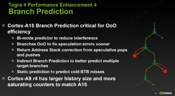
I want to go deeper into ARM’s Cortex A15 but I’ll have to save that for another time. At a high level you’re looking at a much deeper, much wider architecture than the Cortex A9. The integer pipeline is significantly deeper (15 stages vs. 9 stages), however branch prediction has been improved considerably to hopefully offset the difference.
The front end is 50% wider and has double the instruction fetch bandwidth of the Cortex A9, which helps increase instruction level parallelism. In order to capitalize on the 3-wide machine, ARM dramatically increased the size of the reorder buffer and all associated data structures within the machine. While the Cortex A9 could keep around 32 - 40 decoded instructions in its reorder buffer, Cortex A15 can hold 128 - an increase of up to 4x. The larger ROB alone gives you a good idea of the magnitude of difference between the Cortex A9 and A15. While the former was a natural evolution over the Cortex A8, ARM’s Cortex A15 is really a leap forward both in performance and power consumption - clearly aimed at something much more than just smartphones.
Getting to the execution core, A15 continues the trend of being considerably wider than A9. There are more execution ports and more execution units, all of which help to increase ILP/single threaded performance. ARM went to multiple, independent issue queues in order to keep frequencies high. Each issue queue can accept up to three instructions and all issue queues can dispatch in parallel.
The A15 can execute instructions out of order like the A9, however its abilities grow quite a bit. All FP/NEON instructions had to be executed in-order on Cortex A9, but they can now be executed OoO in the A15. Despite the beefier OoO execution engine, the Cortex A15 can’t reorder all memory operations (independent loads can be executed out of order, but stores can’t be completed ahead of loads).
The Cortex A15 moves back to an integrated L2 cache structure, rather than a separate IP block as was the case with the Cortex A9. L1 and L2 cache latencies remain largely unchanged, although I do believe A15 does see a 1 - 2 cycle penalty over A9 in a few cases. The level 2 TLB and other data structures grow in size considerably in order to feed the hungrier machine.
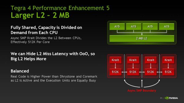
Although the L1 caches remain the same size as NVIDIA’s Cortex A9 (32KB I + 32KB D), the the L2 cache grows to 2MB. The 2MB L2 is shared by all four cores (the companion core has its own private 512KB L2), and any individual core can occupy up to the entire 2MB space on its own. Alternatively, all four cores can evenly share and access the large L2.


75 Comments
View All Comments
xsacha - Saturday, March 23, 2013 - link
Tegra4i uses Cortex-A9. Krait is similar to Cortex-A15. The Krait obviously uses way more power and gives way more performance clock-for-clock. So you are comparing apples and oranges here. The 1.9GHz Krait quad-core is roughly equivalent to 2.5GHz+ in a Tegra 4i.name99 - Monday, February 25, 2013 - link
"But in favor of quad-core: software might start using cores a little more effectively w/time--Google and Apple are apparently trying to make WebKit able to do things like HTML parsing and JavaScript garbage collection in the background, and Microsoft's browser team backgrounds JavaScript compilation"It would be wise to design for the technology we have today, not the dream of technology we may one day have. As I have stated elsewhere, there is ample evidence that on the desktop, even today, multiple threads running on more than two cores at once is very rare. (More precisely
- many apps are multithreaded, but those threads tend to be mostly async IO type threads, mostly waiting
- there is a mild win to having three cores available, but it's not much advantage over two cores
- the situation has improved a little over ten years ago (when the first SMT P4s first started appearing) and when there was little advantage to two cores over one. But most of the improvement is the result of OS vendors moving as much stuff as possible of what they do (GUI, IO, etc) onto the second core.)
The only real code that utilizes multiple cores is video-encoding. In particular both games and photo processing do not use nearly as much multi-core as people imagine.
The situation for mobile is the same, only a little worse because there is less of simultaneous heavyweight apps running.
Given these facts, and the way code is actually structured today, 4 cores makes very little sense.
SMT makes sense, mainly in that its power and area footprint is very low, so it's a win on those occasions when the OS can make use of it. Beyond that, if you have excess transistors available, beefed up vectors (wider registers, and wider units) probably makes more sense. You'll notice that these recommendations parallel what Intel has done over the past few years --- they are not idiots, and desktop code is very similar to mobile code.
As for parallel web browsing, people have been publishing about it for years now; but the real world results remain unimpressive. It remains an unfortunate fact that the things that have been converted to parallel don't seem to be, for most sites, the things that are actually gating performance. A similar problem exists with PDF display (still not as snappy as I would like on an iPad3) --- the simple and obvious things you can imagine for parallelizing the rendering aren't the things that are usually the problem.
In both cases, the ideal situation would be to restart with totally redesigned file formats that are non-serial in nature; but that seems to be a "boil-the-ocean" strategy that no-one wants to commit to yet. (Though it would be nice if Apple and Adobe could get together to redefine a PDF2.0 file format that was explicitly parallel, and that seems rather easier than fixing the web.)
Krysto - Sunday, February 24, 2013 - link
It seems Nvidia really pulled off making Tegra 4's GPU 6x faster than Tegra 3, and with 5 Cortex A15 cores and 6x more GPU cores, all in the same size. Pretty impressive. But still quite disappointing for lack of OpenGL ES 3.0 and OpenCL support. I really hope they plan on supporting them in Tegra 5 along with the new 64 CPU and Maxwell-based GPU cores.Mike1111 - Sunday, February 24, 2013 - link
I would really like to see an analysis/comparison of companion core (Nvidia) vs. big.LITTLE (Samsung).lmcd - Sunday, February 24, 2013 - link
BIG.little (fixed it for ARM) isn't even in reference device stage yet is it?Krysto - Monday, February 25, 2013 - link
No need to fix it. The "opposite" style naming is intentional. It's ironic. Get it?phoenix_rizzen - Monday, February 25, 2013 - link
Exynos 5 Octa, which is A15/A7 big.LITTLE, has been demoed. Tegra 4, which is A15 plus a companion core, has been demoed.Neither are commercially available, neither are in shipping products, neither are available to consumers.
IOW, the Cortex-A15 variations for bit.LITTLE have passed the reference stage, and are in the "find companies to use them to build devices" stage. They'll be in consumers' grubby little hands before Christmas 2013.
tviceman - Sunday, February 24, 2013 - link
GPU performance ended up better than I thought it would after the subdued announcement and leaked early prototype benchmarks. Good to see.wongwarren - Monday, February 25, 2013 - link
I wonder which is faster. This or the Snapdragon 600.varad - Monday, February 25, 2013 - link
Snapdragon 600:http://www.anandtech.com/show/6792/lg-optimus-g-pr...
Tegra 4:
http://www.anandtech.com/show/6787/nvidia-tegra-4-...
So if the metric is simply raw performance [since you asked "faster"], looks like the Tegra 4 will win easily against the Snapdragon 600.
A better/fair comparison would be when we have performance numbers for Snapdragon 600 in a tablet or Tegra 4 in a phone.