Gigabyte Z77X-UP7 Review: OC Oriented Orange Overkill
by Ian Cutress on March 1, 2013 10:30 AM EST- Posted in
- Motherboards
- Intel
- Gigabyte
- Z77
Gigabyte Z77X-UP7 Visual Inspection
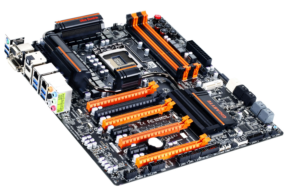
In order to fit the 32 IR3550s onto the Z77X-UP7, as well as the mSATA, OC-Touch buttons, voltage check points and headers, the motherboard is an extra inch wider than standard ATX, also known as E-ATX (305mm x 264mm). The socket area has plenty of space around it for large heatsinks due to the power delivery heatsink being placed slightly further back than usual due to the IR3550s. The 32 phase arrangement is designed in a custom 8x4 rather than 8x2x2, meaning that at any one time 8 phases are operational. It loops around in four cycles to use all 32, 8 at a time, but can use all 32 at once if needed such as for the 2000W power test. This is nothing new in terms of high end power delivery, though 8x2x2 is more common with phases spending one cycle on, one cycle off, rather than one cycle on, three cycles off.
For fan headers, the socket has access to three in immediate reach – a 4-pin CPU fan header above the socket to the right, a 4-pin SYS header above the two 8-pin CPU power connectors on the top left, and a 4-pin SYS fan header between the memory slots and the 24-pin power connector. The other four fan headers are found on the bottom of the board: two 3-pin and two 4-pin, all SYS headers. Ideally I would have liked another CPU header, or one of the bottom headers moved more to the top of the board – for both regular usage and overclocking.
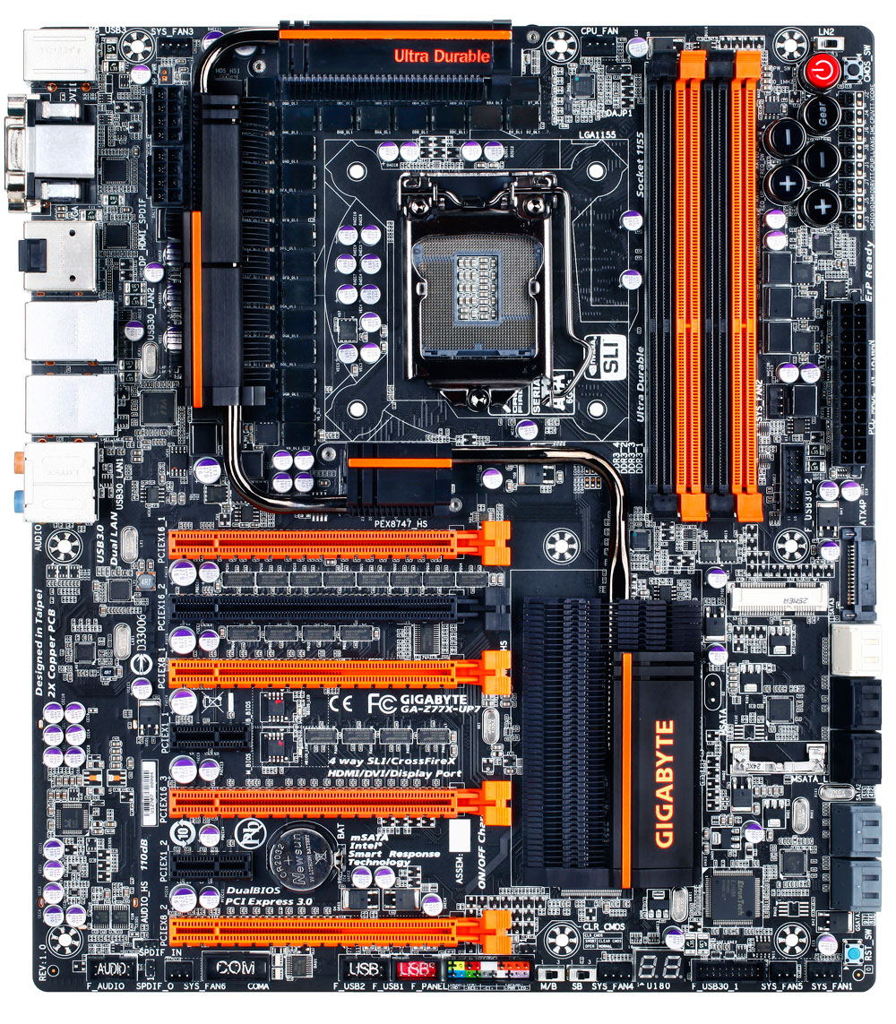
The power delivery heatsink is a vast extended black and orange affair, moving through the phases and VRMs, connected via heatpipe over a PLX 8747 chip and down to the chipset. The PLX chip and chipset come in at ~16W together, although there are very few circumstances that would be taxing both the PCIe lanes and IO (video encoding and file transfer perhaps) at the same time. The heatsink is custom made for the UP7, such that the fins are thin and there are plenty of them, maximizing surface area for airflow in case of large bulky devices (4-way GPUs, LN2 pots) being used. A minor criticism is that when performing sub-zero overclocking, the cold likes to spread around the board, causing more areas for condensation to occur (meaning that good insulation is very important). With a large surface heatsink such as this, it gives plenty of surfaces for condensation to form, and that condensation could roll off of the heatsink onto the motherboard. With that being said, I have not heard of it being an issue so far, but it is theoretically an issue.
Unlike any other Z77 motherboard we have tested at AnandTech, I believe this is the first one on the test bed with two 8-pin power connectors for the CPU. Typically we have a single 8-pin, or an 8-pin and a 4-pin, and the mITX models using a single 4-pin. Sandy Bridge-E requires two 8-pin connectors when pushing the overclocks, but the main reason for the two 8-pins on the UP7 is presumably to cater for the 32 phase power delivery. The board also has a SATA power connector, to give extra juice to the PCIe slots – the PCIe specification says that each slot should provide 75W, however asking for a stable 300W supply from the 24-pin ATX power connector is perhaps asking a little too much. In our testing, to use any of the orange PCIe slots, the SATA power connector had to be used.
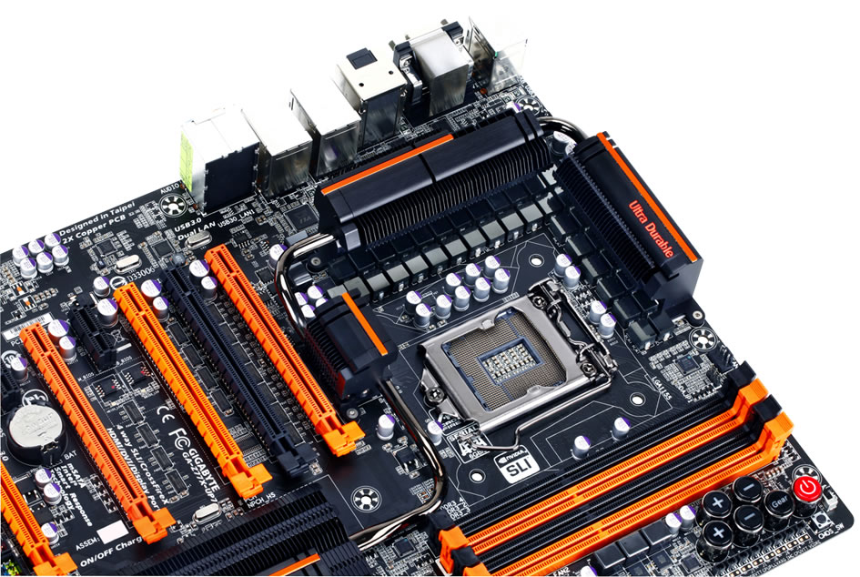
Moving clockwise around the board from the chipset, we have our top right corner full of overclocking utilities. The big red button is a standard Gigabyte power button that distinguishes itself from the ClearCMOS button next to it in both size and visuals such that it is hard to press the wrong one, unlike on some other motherboards. Above the power button is an LN2 mode switch that drops the CPU multiplier down to 16x, ensuring that opening verification programs like CPU-Z does not cause the system to crash.
Below these are a set of five ‘OC-Touch’ buttons, designed to help the user overclock on-the-fly. This allows extreme overclockers to increase the CPU speed during non-CPU intensive tasks, like GPU tests, and reduce it during CPU tasks. The top plus and minus buttons change the CPU ratio, adjusting it by +1 or -1 when pressed. The bottom two buttons change BCLK by 1 MHz, and when the ‘Gear’ button is activated, the buttons adjust BCLK by 0.1 MHz. Unfortunately the bottom row of three buttons do not work out of the box – they only work in the OS and when the OC-Touch driver is installed. Below the OC-Touch buttons are the voltage check points. Users can either directly attach the connections to their multi-meters, or use the plastic adapters supplied in the motherboard box. Each check point comes with its own ground, and all the major voltages are covered – VCore, VTT, IMC, PLL, VDIMM, PCHIO and so on.

Down the right hand side below the OC-Touch is our 24-pin ATX power connector, flanked by a 4-pin fan header, a USB 3.0 header (from the chipset) and a SATA power connector for the VGA ports. The SATA power connector sits above the SATA ports, where we have access to 10 in total – two SATA 6 Gbps and four SATA 3 Gbps from the chipset, then four SATA 6 Gbps from Marvell 9172 controllers. Beside these is an mSATA port, but it shares bandwidth with one of the SATA 3 Gbps, meaning a choice between a SATA port and an mSATA. Each of the chipset ports are RAID 0, 1, 5 and 10 capable, whereas the Marvell SATA ports are only RAID 0 and 1.
Along the bottom of the motherboard, from right to left, the system provides a reset button, two fan headers, a USB 3.0 header powered by an Etron EJ168 controller, a two-digit debug LED, another header, then two BIOS switches. These switches deal with the DualBIOS system – one switch selects either BIOS one or two, while the other enables and disables BIOS recovery. The latter can be important when overclocking, should the motherboard want to initiate BIOS recovery after several failed overclock attempts but the user wants to tweak the settings more. Moving along the left of the board form the switches is the front panel header, two USB 2.0 headers (one of which supports QuickCharge), a COM header, a final fan header, and front panel audio powered by a Realtek ALC898. Two points are worth noting – this is the first Gigabyte motherboard in a while I have seen without a TPM header, and the Realtek ALC898 is a dichotomous choice of codec on a $400 motherboard. On the one hand to appeal to anyone other than overclockers, getting something better on board would be a good selling point given the price bracket, whereas overclockers would prefer it removed altogether.
In the overview to this review I remarked on the PCIe configuration being something slightly different. We have a system that uses a PLX 8747 chip to output 32 PCIe 3.0 lanes to any number of PCIe slots, while taking in either 8 or 16 PCIe 3.0 lanes from the CPU. We have seen both examples in our four-board PLX 8747 review back in August 2012. Ideally we do not want the chip as it adds some extra overhead – we would rather have the lanes straight from the CPU itself. But the Z77 specifications only allow up to an x8/x4/x4 distribution of the 16 CPU lanes, which potentially limits bandwidth and denies 4-way PCIe setups. With the PLX, we can do a full PLX setup (x8/x8/x8/x8), or only send 8 lanes to the PLX and keep 8 lanes for the first PCIe slot (giving x16/x8/x8/x8) but limiting GPUs 2, 3 and 4 in upload bandwidth. Gigabyte instead use switches to send the PCIe lanes around – when one GPU is being used, put it in the black slot for x16 PCIe 3.0 from the CPU, bypassing the PLX chip. When we use more GPUs, the orange slots have to be used, which have a full PLX layout (up to x8/x8/x8/x8). In crude MSPaint notation:
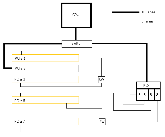
Starting at the CPU, it sends 16 PCIe lanes down to a switch – the lanes can either all go to PCIe 2 for optimal single GPU performance, or to the PLX chip for multi-GPU layouts. When at the PLX chip, we get 32 lanes to play with (see our original PLX 8747 review for reasons why), which are all sent out in sets of eight. Set 1 goes to PCIe 1 and Set 3 goes to PCIe 5. Set 2 encounters a switch – if there is a device in PCIe 3, it goes there, otherwise to PCIe 1. Set 4 does likewise – if there is a device in PCIe 7, it goes there, otherwise to PCIe 5. Sounds complicated, but it allows for the best lane allocation for up to four devices.
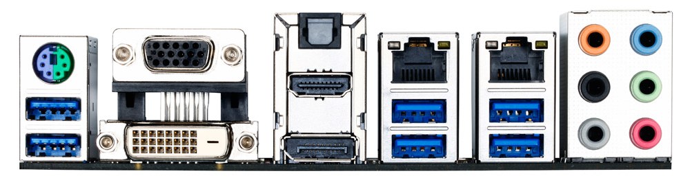
The rear IO is a little odd, considering the market segment for the UP7. The motherboard is built for multi-GPU setups, and thus it makes little sense to include every video output the integrated GPU offers. The sole explanation I could suggest would be that Gigabyte could not route any more USB 2.0 ports up to the rear IO without adding extra PCB layers or compromising speed. Nevertheless, I would imagine the video outputs rarely being used except for quick testing. From left to right, we get a combination PS/2 port, two USB 3.0 (VIA), D-Sub, DVI-D, HDMI, DisplayPort, optical SPDIF output, two gigabit Ethernet ports (one Intel, one Atheros), two more USB 3.0 from VIA, two USB 3.0 from the chipset, and audio ports. Note that in the manual, it states the first two USB 3.0 ports (left to right) are from the chipset – this is wrong and it is the two USB 3.0 ports on the right. Place your keyboard and mouse here to avoid driver issues before installing the VIA USB 3.0 drivers.
Board Features
| Gigabyte Z77X-UP7 | |
| Price | Link |
| Size | E-ATX (305mm x 264mm) |
| CPU Interface | LGA-1155 |
| Chipset | Intel Z77 |
| Memory Slots |
Four DDR3 DIMM slots supporting up to 32 GB Up to Dual Channel, 1066-2800 MHz |
| Video Outputs |
D-Sub DVI-D HDMI DisplayPort |
| Onboard LAN |
Intel 82579V Atheros AR8161/8165 GC-WB300D Dual Band 802.11b/g/n WiFi PCIe x1 Card |
| Onboard Audio | Realtek ALC898 |
| Expansion Slots |
1 x PCIe 3.0 x16 4 x PCIe 3.0 x16 via PLX 8747 - x16/-/x16x/- - x8/x8/x16/- - x8/x8/x8/x8 2 x PCIe 2.0 x1 |
| Onboard SATA/RAID |
2 x SATA 6 Gbps (Chipset), RAID 0, 1, 5, 10 4 x SATA 3 Gbps (Chipset), RAID 0, 1, 5, 10 4 x SATA 6 Gbps (Marvell 8172), RAID 0, 1 1 x mSATA 3 Gbps (Chipset, shares with SATA port) |
| USB |
4 x USB 3.0 (Chipset) [2 onboard, 2 rear panel] 4 x USB 3.0 (VIA VL800) [4 rear panel] 2 x USB 3.0 (Etron EJ168) [2 onboard] 4 x USB 2.0 (Chipset) [4 onboard] |
| Onboard |
6 x SATA 6 Gbps 4 x SATA 3 Gbps 1 x mSATA 3 Gbps 2 x USB 3.0 Headers 2 x USB 2.0 Headers 7 x Fan Headers 1 x Front Panel Audio Header 1 x Front Panel Header 1 x COM Header Power/Reset/ClearCMOS Buttons Two Digit Debug OC Touch Buttons Voltage Measurement Points BIOS Switches LN2 Switch |
| Power Connectors |
1 x 24-pin ATX Power Connector 2 x 8-pin CPU Power Connector 1 x SATA Power Connector for VGA |
| Fan Headers |
1 x CPU (4-pin) 6 x SYS (4x4-pin, 2x3-pin) |
| IO Panel |
1 x Combination PS/2 Port 4 x USB 3.0 (VIA) D-Sub DVI-D HDMI DisplayPort Optical SPDIF Output 2 x GbE NIC (Intel, Atheros) 2 x USB 3.0 (Chipset) Audio Jacks |
| Warranty Period | 3 Years |
| Product Page | Link |
Aside from the power delivery, the main competition the Z77X-UP7 has is with the G1.Sniper 3. The UP7 gets the overclocking features, such as OC Touch, the single PCIe slot not attached to the PLX and fan headers, whereas the G1. Sniper3 has Core3D Audio, a Killer NIC, TPM and a PCI slot. The rest of the package is much the same, although there are no UP7 specific add-ons, like with ASRock Z77 OC Formula which included some standoffs for overclocking and a themed back to keep all the bits in.
If we compare to the Z77 OC Formula, the Z77X-UP7 has more NICs, an mSATA port, 4-way GPU support, more IGP video outputs, a bundled WiFi card, two more USB 3.0 ports (at the expense of 6 USB 2.0 ports), an LN2 switch and the CPU power delivery (not to mention the additional VGA comes from a SATA port rather than a molex). On the other hand, the Z77 OC Formula has a combo air/water VRM heatsink, PCIe switches, more USB ports on the rear IO, one more fan header than the UP7 (even though it is occupied), and a selection of BIOS/software that is miles easier to use (more on that later).


41 Comments
View All Comments
Drasca - Saturday, May 4, 2013 - link
I am really getting annoyed at the insufficient documentation on PCI-E slot configurations being enabled/disabled. It makes testing a lot more difficult. Just tried orange slots 1 and 2, thinking they'd work. Nope. Tried a single card in slot 2 orange. Nope. It is likely disabled on default. There is no mention of this in the very short multi language manual Gigabyte provides. I've tried the Asus Maximus V Extreme a few weeks ago, and while I didn't know about it-- at least the thing provided a configuration card and table documented in the depths of its manual. No such documentation is provided by Gigabyte.Time to try population all slots at once.