The ARM vs x86 Wars Have Begun: In-Depth Power Analysis of Atom, Krait & Cortex A15
by Anand Lal Shimpi on January 4, 2013 7:32 AM EST- Posted in
- Tablets
- Intel
- Samsung
- Arm
- Cortex A15
- Smartphones
- Mobile
- SoCs
Late last month, Intel dropped by my office with a power engineer for a rare demonstration of its competitive position versus NVIDIA's Tegra 3 when it came to power consumption. Like most companies in the mobile space, Intel doesn't just rely on device level power testing to determine battery life. In order to ensure that its CPU, GPU, memory controller and even NAND are all as power efficient as possible, most companies will measure power consumption directly on a tablet or smartphone motherboard.
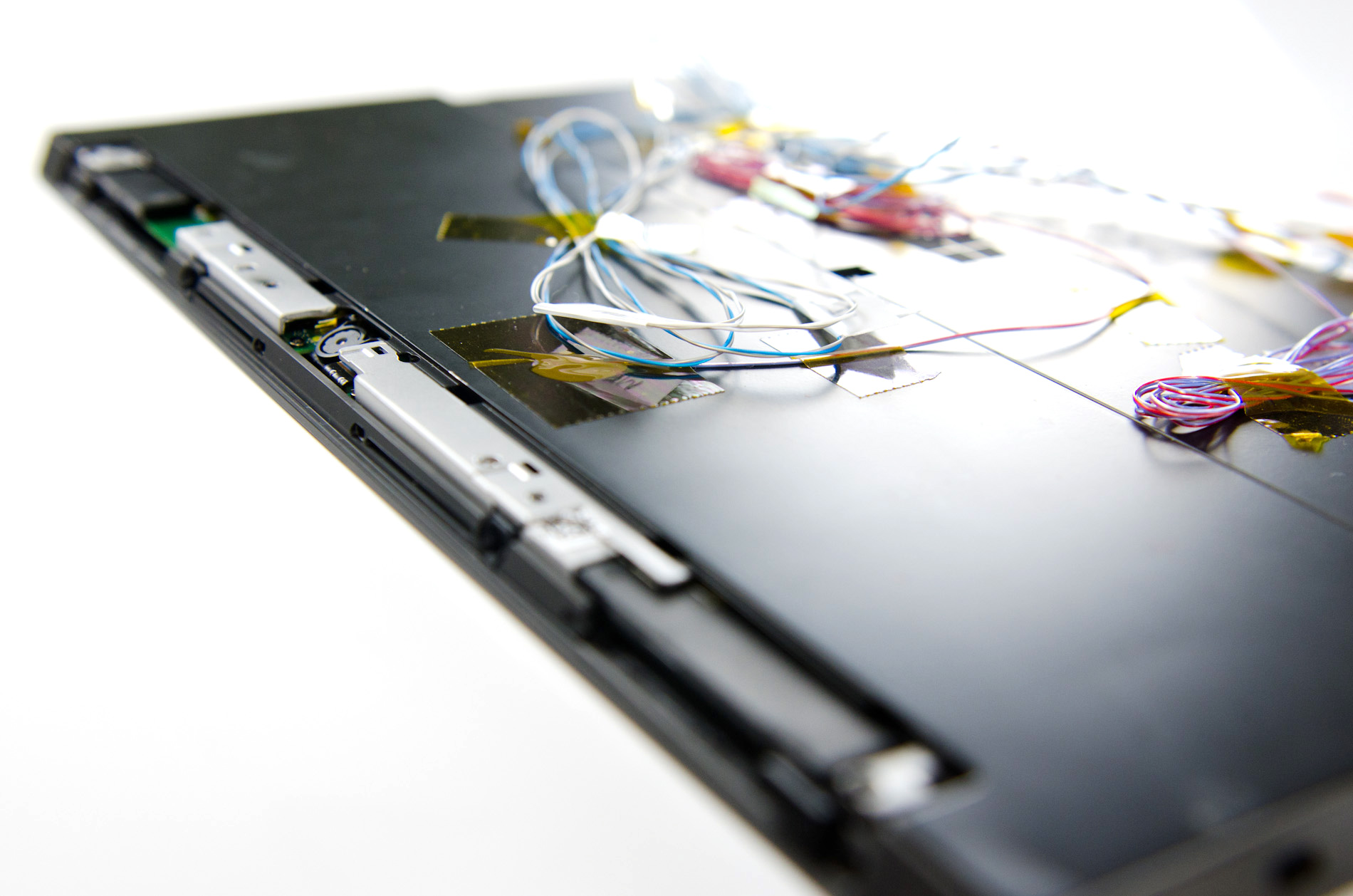
The process would be a piece of cake if you had measurement points already prepared on the board, but in most cases Intel (and its competitors) are taking apart a retail device and hunting for a way to measure CPU or GPU power. I described how it's done in the original article:
Measuring power at the battery gives you an idea of total platform power consumption including display, SoC, memory, network stack and everything else on the motherboard. This approach is useful for understanding how long a device will last on a single charge, but if you're a component vendor you typically care a little more about the specific power consumption of your competitors' components.
What follows is a good mixture of art and science. Intel's power engineers will take apart a competing device and probe whatever looks to be a power delivery or filtering circuit while running various workloads on the device itself. By correlating the type of workload to spikes in voltage in these circuits, you can figure out what components on a smartphone or tablet motherboard are likely responsible for delivering power to individual blocks of an SoC. Despite the high level of integration in modern mobile SoCs, the major players on the chip (e.g. CPU and GPU) tend to operate on their own independent voltage planes.
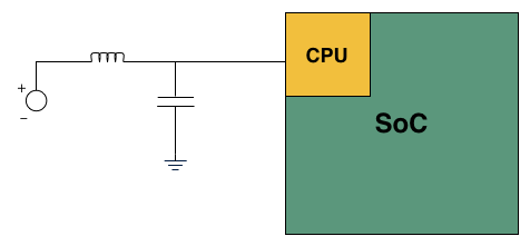
A basic LC filter
What usually happens is you'll find a standard LC filter (inductor + capacitor) supplying power to a block on the SoC. Once the right LC filter has been identified, all you need to do is lift the inductor, insert a very small resistor (2 - 20 mΩ) and measure the voltage drop across the resistor. With voltage and resistance values known, you can determine current and power. Using good external instruments (NI USB-6289) you can plot power over time and now get a good idea of the power consumption of individual IP blocks within an SoC.
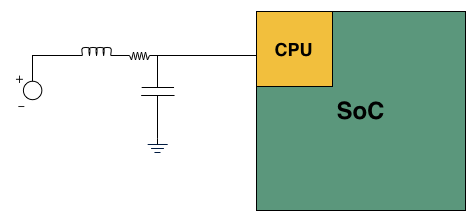
Basic LC filter modified with an inline resistor
The previous article focused on an admittedly not too interesting comparison: Intel's Atom Z2760 (Clover Trail) versus NVIDIA's Tegra 3. After much pleading, Intel returned with two more tablets: a Dell XPS 10 using Qualcomm's APQ8060A SoC (dual-core 28nm Krait) and a Nexus 10 using Samsung's Exynos 5 Dual (dual-core 32nm Cortex A15). What was a walk in the park for Atom all of the sudden became much more challenging. Both of these SoCs are built on very modern, low power manufacturing processes and Intel no longer has a performance advantage compared to Exynos 5.
Just like last time, I ensured all displays were calibrated to our usual 200 nits setting and ensured the software and configurations were as close to equal as possible. Both tablets were purchased at retail by Intel, but I verified their performance against our own samples/data and noticed no meaningful deviation. Since I don't have a Dell XPS 10 of my own, I compared performance to the Samsung ATIV Tab and confirmed that things were at least performing as they should.
We'll start with the Qualcomm based Dell XPS 10...


140 Comments
View All Comments
A5 - Friday, January 4, 2013 - link
Even if you just look at the Sunspider (which draws nothing on the screen) power draw, it's pretty clear that the A15 draws more power. There have been a ton of OEMs complaining about A15's power draw, too.madmilk - Friday, January 4, 2013 - link
Since when did screen resolution matter for CPU power consumption on CPU benchmarks? Platform power might change, yes, but this doesn't invalidate many facts like Cortex-A15 using twice as much power on average compared to Krait, Atom or Cortex-A9.Wolfpup - Friday, January 4, 2013 - link
Good lord. Do you have some evidence for any of this? If neither Windows nor Android is the "right platform" for ARM, then...are you waiting for Blackberry benchmarks? That's a whole lot of spin you're doing, presumably to fit the data to your preconceived "ARM IS BETTER!" faith.Veteranv2 - Friday, January 4, 2013 - link
Hahaha, the Nexus 10 has almost 4 times the pixels of the Atom.And the conclusion is it draws more power in benchmarks? Of course, those pixels aren't going to fill itself. Way to make conclusion.
How big was that Intel PR cheque?
iwod - Saturday, January 5, 2013 - link
While i wouldn't say it was a Intel PR, I think they should definitely have left the system level power usage out of the questions. There is no point telling me that a 100" Screen with ARM is using X amount of power compared to 1" Screen with Haswell.It is confusing.
But they did include CPU and GPU benchmarks. So saying it is Intel PR is just trolling.
AlB80 - Friday, January 4, 2013 - link
Architectures with variable length of instruction are doomed. Actually there is only one remains. x86.Intel made the step into a happy past when CISC has an advantage over RISC, when superscalarity was just a theory.
Cortex A57 is coming. ARM cores will easily outperform Atom by effective instruction rate with minimum overhead.
Wolfpup - Friday, January 4, 2013 - link
How is x86 doomed when it has an absolute stranglehold on real PCs, and is now competitive on ultramobile platforms?The only disadvantage it holds is the need for a larger decoder on the front end, which has been proportionally shrinking since 1995.
djgandy - Friday, January 4, 2013 - link
plus effing one!I think some people heard their uni lecturers say something once in 1999 and just keep repeating it as if it is still true!
AlB80 - Friday, January 4, 2013 - link
Shrinking decoder... nice myth. Of course complicated scheduler and ALU dozen impact on performance, but do not forget how decoded instruction queues are filled. Decoder is only one real difference.1. There is fundamental limits how many variable instructions can be decoded per clock. CISC has an instruction cross-interference at the decoder stage. One logical block should determine a total length of decoded instructions.
2. There is a trick when CISC decoder is disintegrated into 2-3 parts with dedicated inputs, so its looks like a few independent decoders, but each part can not decode any instruction.
Now compare it with RISC.
And as I said, what happens when Cortex can decode 4,5,6,7,8 instructions?
Kogies - Friday, January 4, 2013 - link
Don't be so quick to prophesy the death of a' that. What happens when a Cortex decodes 8 instructions... I don't know, it uses 8W?Also, didn't Apple choose CISC (Intel) chips over RISC (PowerPC)? Interestingly, I believe Apple made the switch to Intel because the PowerPC chips had too high a power premium for mobile computers.