The ARM vs x86 Wars Have Begun: In-Depth Power Analysis of Atom, Krait & Cortex A15
by Anand Lal Shimpi on January 4, 2013 7:32 AM EST- Posted in
- Tablets
- Intel
- Samsung
- Arm
- Cortex A15
- Smartphones
- Mobile
- SoCs
Modifying a Krait Platform: More Complicated
Modifying the Dell XPS 10 is a little more difficult than Acer's W510 and Surface RT. In both of those products there was only a single inductor in the path from the battery to the CPU block of the SoC. The XPS 10 uses a dual-core Qualcomm solution however. Ever since Qualcomm started doing multi-core designs it has opted to use independent frequency and voltage planes for each core. While all of the A9s in Tegra 3 and both of the Atom cores used in the Z2760 run at the same frequency/voltage, each Krait core in the APQ8060A can run at its own voltage and frequency. As a result, there are two power delivery circuits that are needed to feed the CPU cores. I've highlighted the two inductors Intel lifted in orange:
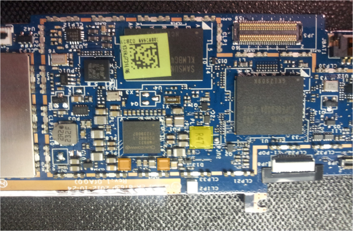
Each inductor was lifted and wired with a 20 mΩ resistor in series. The voltage drop across the 20 mΩ resistor was measured and used to calculate CPU core power consumption in real time. Unless otherwise stated, the graphs here represent the total power drawn by both CPU cores.
Unfortunately, that's not all that's necessary to accurately measure Qualcomm CPU power. If you remember back to our original Krait architecture article you'll know that Qualcomm puts its L2 cache on a separate voltage and frequency plane. While the CPU cores in this case can run at up to 1.5GHz, the L2 cache tops out at 1.3GHz. I remembered this little fact late in the testing process, and we haven't yet found the power delivery circuit responsible for Krait's L2 cache. As a result, the CPU specific numbers for Qualcomm exclude any power consumed by the L2 cache. The total platform power numbers do include it however as they are measured at the battery.
The larger inductor in yellow feeds the GPU and it's instrumented using another 20 mΩ resistor.
Visualizing Krait's Multiple Power/Frequency Domains
Qualcomm remains adament about its asynchronous clocking with multiple voltage planes. The graph below shows power draw broken down by each core while running SunSpider:
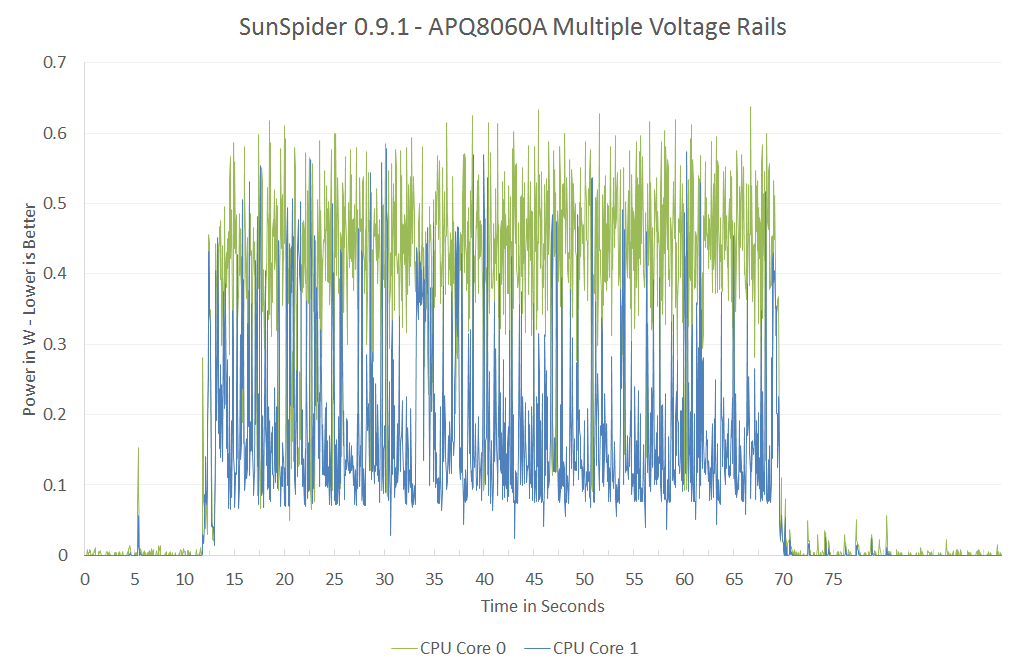
SunSpider is a great benchmark to showcase exactly why Qualcomm has each core running on its own power/frequency plane. For a mixed workload like this, the second core isn't totally idle/power gated but it isn't exactly super active either. If both cores were tied to the same voltage/frequency, the second core would have higher leakage current than in this case. The counter argument would be that if you ran the second core at its max frequency as well it would be able to complete its task quicker and go to sleep, drawing little to no power. The second approach would require a very fast microcontroller to switch between v/f modes and it's unclear which of the two would offer better power savings. It's just nice to be able to visualize exactly why Qualcomm does what it does here.
On the other end of the spectrum however is a benchmark like Kraken, where both cores are fairly active and the workload is balanced across both cores:
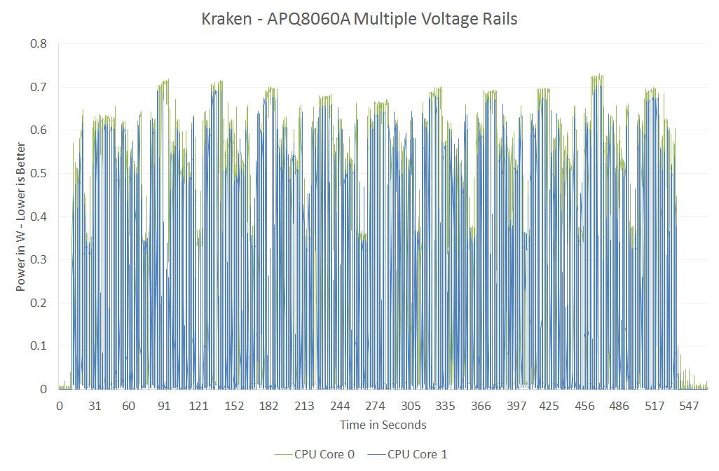
Here there's no real benefit to having two independent voltage/frequency planes, both cores would be served fine by running at the same voltage and frequency. Qualcomm would argue that the Kraken case is rare (single threaded performance still dominates most user experience), and the power savings in situations like SunSpider are what make asynchronous clocking worth it. This is a much bigger philosophical debate that would require far more than a couple of graphs to support and it's not one that I want to get into here. I suspect that given its current power management architecture, Qualcomm likely picked the best solution possible for delivering the best possible power consumption. It's more effort to manage multiple power/frequency domains, effort that I doubt Qualcomm would put in without seeing some benefit over the alternative. That being said, what works best for a Qualcomm SoC isn't necessarily what's best for a different architecture.


140 Comments
View All Comments
Kidster3001 - Friday, January 4, 2013 - link
Samsung uses everyone's chips in their phones. Samsung, Qualcomm, TI... everyone's. I would not be surprised to see a Samsung phone with Atom in it eventually.jeffkibuule - Friday, January 4, 2013 - link
They've never used other non-Samsung SoCs by choice, especially in their high end phones. They only used Qualcomm MSM8960 in the US GS III because Qualcomm's separate baseband MDM9615 wasn't ready. As soon as it was, we saw the Galaxy Note II use Exynos again. Nvidia and TI chips have been used in the low end from Samsung, but that's not profitable to anyone.Intel needs a major design win from a tier one OEM willing to put its chip inside their flagship phone, and with most phone OEMs actually choosing to start designing their own ARM SoCs (including even LG and Huawei), that task is getting a lot harder than you might think.
felixyang - Saturday, January 5, 2013 - link
some versions of Samsung's GS2 use TI's OMAP.iwod - Saturday, January 5, 2013 - link
Exactly like what is said above. If they have a choice they would rather use everything they produce themselves. Simply Because Wasted Fabs Space is expensive.Icehawk - Friday, January 4, 2013 - link
I find these articles very interesting - however I'd really like to see an aggregate score/total for power usage, IOW what is the area under the curve? As discussed being quicker to complete at higher power can be more efficient - however when looking at a graph it is very hard to see what the total area is. Giving a total wattage used during the test (ie, area under curve) would give a much easier metric to read and it is the important #, not what the voltage maxes or minimums at but the overall usage over time/process IMO.extide - Friday, January 4, 2013 - link
There are indeed several graphs that display total power used in joules, which is the area under the curve of the watts graphs. Maybe you missed them ?jwcalla - Friday, January 4, 2013 - link
That's what the bar charts are showing.GeorgeH - Friday, January 4, 2013 - link
It's already there. A Watt is a Joule/Second, so the area under the power/time graphs is measured in Watts * Seconds = Joules.Veteranv2 - Friday, January 4, 2013 - link
Another Intel PR Article, it is getting really sad on this website.Now since you are still using Win8 which is garbage for ARM. Please us the correct software platform for ARM chips. I'd love to see those power measurements then.
Anandtech did it again. Pick the most favorable software platform for Intel, give the least favorable to ARM.
Way to go! Again....
Intel PR at its best...
Veteranv2 - Friday, January 4, 2013 - link
Oh wait its even better!They used totally different screens with almost 4 times the pixels on the nexus 10 and then says it requires more power to do benchmarks. Hahaha, this review gave me a good laugh. Even worse then the previous ones.
This might explain the lack of product overviews at the start.