Gigabyte GA-7PESH1 Review: A Dual Processor Motherboard through a Scientist’s Eyes
by Ian Cutress on January 5, 2013 10:00 AM EST- Posted in
- Motherboards
- Gigabyte
- C602
Visual Inspection
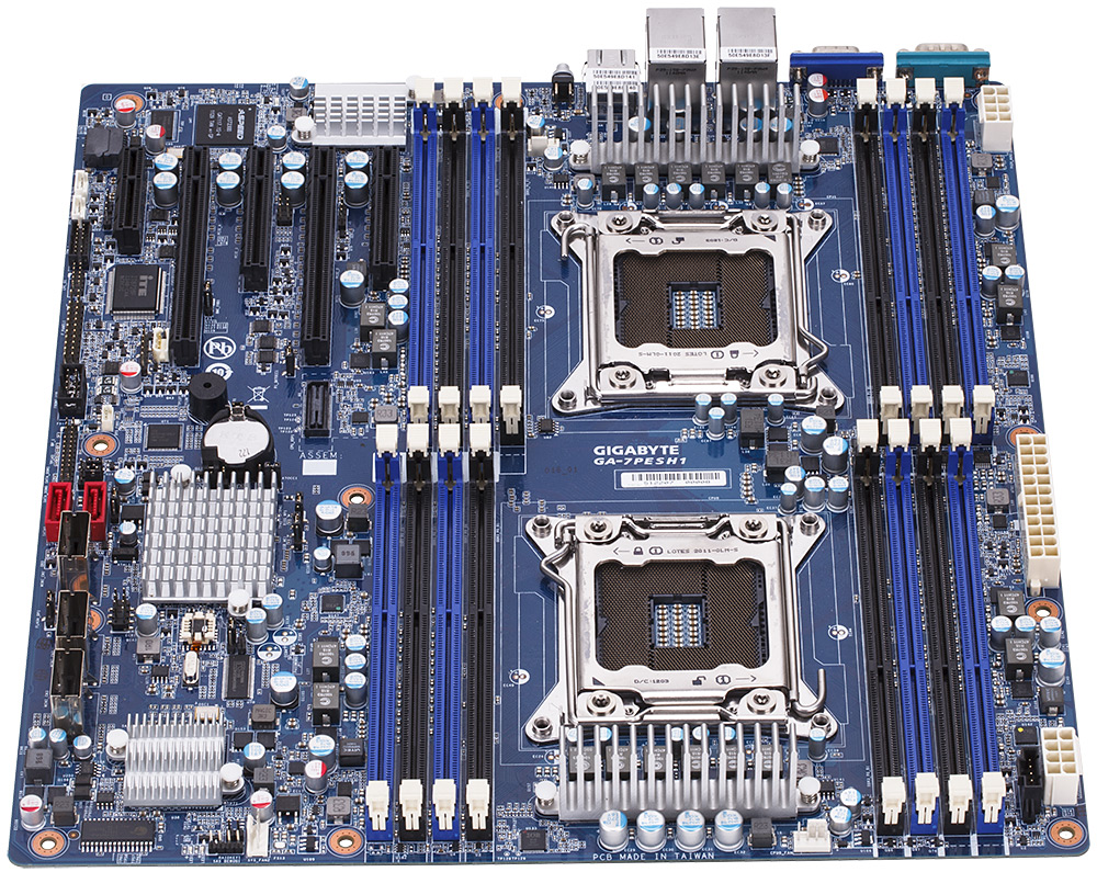
I knew server boards were large, but coming from the ATX and E-ATX standards, this thing is huge. It measures 330mm x 305mm (13” x 12”) which correlates to the SSI EEB specification for server motherboards. This is the size exact size of an official E-ATX motherboard (despite a small amount of loose definition), but to put the icing on the cake, the mounting holes for the motherboard are different to the normal ATX standards. If we took a large case, like the Rosewill Blackhawk-Ultra, it supports ATX, SSI CEB, XL-ATX, E-ATX and HPTX, up to 13.6” x 15”, but not SSI EEB. Thus drilling extra holes for standoffs may be required.
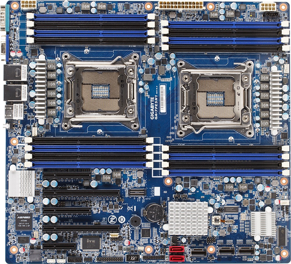
Unlike the SR-X or Z9PE-D8 WS, the GA-7PESH1 supports two memory modules per channel for all channels on board. In terms of specifications this means support for up to 128 GB UDIMM (i.e. regular DDR3), 128 GB UDIMM ECC, and 512 GB RDIMM ECC. Due to the nature of the design, only 1066-1600 MHz is supported, but the GA-7PESH1 supports 1600 MHz when all slots are populated. For our testing, Kingston has kindly supplied us with 8x4GB of their 1600 C11 ECC memory.
As with the majority of server boards, stability and longevity is a top priority. This means no overclocking, and Gigabyte can safely place a six phase power delivery on each CPU – it also helps that all SB-E Xeons are multiplier locked and there is no word of unlocked CPUs being released any time soon. As we look at the board, standards dictate that the CPU on the right is designated as the first CPU. Each CPU has access to a single fan header, and specifications for coolers are fairly loose in both the x and the y directions, limited only by memory population and the max z-height of the case or chassis the board is being placed into. As with all dual CPU motherboards, each CPU needs its own Power Connector, and we find them at the top of the board behind the memory slots and at opposite ends. The placement of these power connectors is actually quite far away for a normal motherboard, but it seems that the priority of the placement is at the edge of the board. In between the two CPU power connectors is a standard 24-pin ATX power connector.
One of the main differences I note coming from a consumer motherboard orientation is the sheer number of available connectors and headers on such a server motherboard. For example, the SATA ports have to be enabled by moving the jumpers the other side of the chipset. The chipset heatsink is small and basic – there is no need for a large heatsink as the general placement for such a board would be in a server environment where noise is not particularly an issue if there are plenty of Delta fans to help airflow.
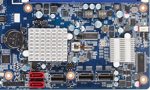
On the bottom right of the board we get a pair of SATA ports and three mini-SAS connections. These are all perpendicular to the board, but are actually in the way of a second GPU being installed in a ‘normal’ motherboard way. Users wishing to use the second PCIe x8 slot on board may look into PCIe risers to avoid this situation. The heatsink on the right of this image covers up an LSI RAID chip, allowing the mSAS drives to be hardware RAIDed.
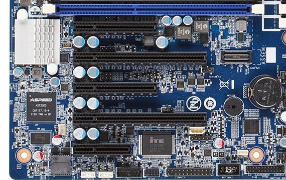
As per normal operation on a C602 DP board, the PCIe slots are taken from the PEG of one CPU. On some other boards, it is possible to interweave all the PCIe lanes from both CPUs, but it becomes difficult when organizing communication between the GPUs on different CPUs. From top to bottom we get an x8 (@x4), x16, x8 (@x4), x16 (@x8), x4(@x1). It seems odd to offer these longer slots at lower speed ratings, but all of the slots are Gen 3.0 capable except the x4(@x1). The lanes may have been held back to maintain data coherency.
To those unfamiliar with server boards, of note is the connector just to the right of center of the picture above. This is the equivalent of the front panel connection on an ATX motherboard. At almost double the width it has a lot more options, and where to put your cables is not printed on the PCB – like in the old days we get the manual out to see what is what.
On the far left we have an ASPEED AST2300 chip, which has multiple functions. On one hand it is an onboard 2D graphics chip which powers the VGA port via its ARM926EJ (ARM9) core at 400 MHz. For the other, it as an advanced PCIe graphics and remote management processor, supporting dual NICs, two COM ports, monitoring functions and embedded memory. Further round this section gives us a removable BIOS chip, a COM header, diagnostic headers for internal functions, and a USB 2.0 header.
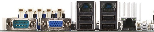
The rear IO is very bare compared to what we are normally used to. From left to right is a serial port, the VGA port, two gigabit Ethernet NICs (Intel I350), four USB 2.0 ports, the KVM server management port, and an ID Switch button for unit identification. There is no audio here, no power/reset buttons, and no two-digit debug LED. It made for some rather entertaining/hair removing scenarios when things did not go smoothly during testing.
Board Features
| Gigabyte GA-7PESH1 | |
| Price |
Contact: 17358 Railroad St. City of Industry CA 91748 +1-626-854-9338 |
| Size | SSI EEB |
| CPU Interface | LGA 2011 |
| Chipset | Intel C602 |
| Memory Slots |
Sixteen DDR3 DIMM slots supporting: 128GB (UDIMM) @ 1.5V 512GB (RDIMM) @ 1.5V 128GB DDR3L @ 1.35 V Quad Channel Arcitecture ECC RDIMM for 800-1600 MHz Non-ECC UDIMM for 800-1600 MHz |
| Video Outputs | VGA via ASPEED 2300 |
| Onboard LAN | 2 x Intel I350 supporting uo to 1000 Mbps |
| Onboard Audio | None |
| Expansion Slots |
1 x PCIe 3.0 x16 1 x PCIe 3.0 x16 (@ x8) 2 x PCIe 3.0 x8 (@ x4) 1 x PCIe 2.0 x4 (@ x1) |
| Onboard SATA/RAID |
2 x SATA 6 Gbps, Supporting RAID 0,1 2 x mini-SAS 6 Gbps, Supporting RAID 0,1 1 x mini-SAS 3 Gbps, Supporting RAID 0,1 |
| USB | 6 x USB 2.0 (Chipset) [4 back panel, 2 onboard] |
| Onboard |
2 x SATA 6 Gbps 2 x mSAS 6 Gbps 1 x mSAS 3 Gbps 1 x USB 2.0 Header 4 x Fan Headers 1 x PSMI header 1 x TPM header 1 x SKU KEY header |
| Power Connectors |
1 x 24-pin ATX Power Connector 2 x 8-pin CPU Power Connector |
| Fan Headers |
2 x CPU (4-pin) 2 x SYS (4-pin, 3-pin) |
| IO Panel |
1 x Serial Port 1 x VGA 2 x Intel I350 NIC 4 x USB 2.0 1 x KVM NIC 1 x ID Switch |
| Warranty Period | Refer to Sales |
| Product Page | Link |
Without having a direct competitor to this board on hand there is little we can compare such a motherboard to. In this level having server grade Intel NICs should be standard, and this board can take 8GB non-ECC memory sticks or 32GB ECC memory sticks, for a maximum of 512 GB. If your matrix solvers are yearning for memory, then this motherboard can support it.


64 Comments
View All Comments
dj christian - Monday, January 14, 2013 - link
No please!This article should be a one time only or once every 2 years at most.
nadana23 - Sunday, January 6, 2013 - link
From the looks of results some of the benchmarks are HIGHLY sensitive to effective bandwidth per thread (ie, GDDR5 feeding a GPU stream processor >> DDR3 feeding a Xeon HT core).However - it must be noted that 8x DIMMS is insufficient to achieve full memory bandwidth on Xeon E5 2S!
I'd suggest throwing a pure memory bandwidth test into the mix to make sure you're actually getting the rated number (51.2GB/s)...
http://ark.intel.com/products/64596/Intel-Xeon-Pro...
... as I strongly suspect your memory config is crippling results.
Dell's 12G config guidelines are as good a place as any to start on this :-
http://en.community.dell.com/cfs-file.ashx/__key/c...
Simply removing one E5-2590 and moving to 1-Package, 8 DIMM config may (counter-intuitively) bench(market) faster... for you.
dapple - Sunday, January 6, 2013 - link
Great article, thanks! This is the sort of benchmark I've been wanting to see for quite some time now - simple, brute-force numerics where the code is visible and straightforward. Too many benchmarks are black boxes with processor- and compiler-specific tunes to make manufacturer "X" appear superior to "Y". That said, it would be most illustrative to perform a similar 'mark using vanilla gcc on both MS and *nix OS.daosis - Sunday, January 6, 2013 - link
It is long known issue, when windows does not start after changing hardware, especially GPU (not always so). There is as long known trick so. Just before last "power off" one should replace GPU's own driver with basic microsoft's one. In case of GPU it is "standart Vga adapter" (device manager - update driver - browse my computer - let me pick up). In fact one can replace all specific drivers on OS with similiar basic from MS and then to put this hard drive virtually to any system without any need for fresh install. Mind you, that after first boot it takes some time for OS to find and install specific drivers.jamesf991 - Sunday, January 6, 2013 - link
In the early '70s I was doing very similar simulations using a PDP 11/40 minicomputer. (I can send citations to my publications if anyone is interested.) At Texas Tech and later at Caltech, I simulated systems involving heterogeneous electron transfer kinetics, various chemical reactions in solution, coulostatics, galvanostatics, voltammetry, chronocoulometry, AC voltammetry, migration, double layer effects, solution hydrodynamics (laminar only), etc. Much of this was done on a PDP 11/40, originally with 8K words (= 16K bytes) of core memory. Later the machine was upgraded to 24 K words (!), we got a floating point board, and a hard disk drive (5 M words, IIRC). My research director probably paid in excess of $50K for the hardware. One cute project was to put a simulation "inside" a nonlinear regression routine to solve for electrode kinetic parameters such as k and alpha. Each iteration of the nonlinear solver required a new simulation -- hand-coding the innermost loops using floating point assembly instructions was a big speedup!I wonder how the old PDP would stack up against the 3770?
flynace - Monday, January 7, 2013 - link
Do you guys think that once Haswell moves the VRM on package that someone might do a 2 socket mATX board?Even if it means giving up 2 of the 4 PCIe slots and/or 2 DIMMs per socket it would be nice to have a high core count standard SFF board for those that need just that.
samsp99 - Monday, January 7, 2013 - link
I found this review interesting, but I don't think this board is really targeted at the HPC market. It seems like it would be good as part of a 2U / 12 + 2 drive system, similar to the Dell C2100. It would make a good virtual host, SQL, active web server etc. Having the 3 mSAS connectors would enable 4 drive each without the need for a SAS expander.Servers are designed for 99.999% uptime, remote management, and hands-off operation. To achieve that you need redundent power, UPS, Networking, storage etc. They also require high airflow, which is noisy and not something you want sitting under your desk. Based on that, it makes sense that the MB is intended for sale to system builders not your general build your own enthusiast.
HW manufactuerers are faced with a similar problem to airlines - consumers gravitate to the cheapest price, and so the only real money to be made is selling higher profit margin products to businesses. Servers are where intel etc makes their profits.
For the computational problems the author is trying to solve, to me it would seem to be better to consider:
a) At one point, I think google was using commodity hardware, with custom shelving etc. Assuming the algorithms can be paralleled on different hosts, you shouldn't need the reliability of traditional servers, so why not use a number of commodity systems together, choosing the components that have the best perf/$.
b) There are machines designed for HPC scenarios, such as HPC Systems E5816 that supports 8x Xeon E7-8000 (10 core) processors, or the E4002G8 - that will take 8 nVidia Tesla cards.
c) What about developing and testing the software on cheap worstations, and then when you are sure its ready, buying compute time from Amazon cloud services etc.
babysam - Monday, January 7, 2013 - link
It is quite delighting to look at your review on Anandtech (especially when I am using software and computer configurations of similar nature for my studies), as it is quite difficult for me to evaluate the performance gain of "real-life" software (i.e. science oriented in my case) on new hardware before buying.From what I have seen in your code segments provided (especially for the n-body simulation part) , there are large amount of floating-point divisions. Is there any possibility that the code is not only limited by the cache size(and thrashing), but by the limited throughput of the floating-point divider? (i.e. The performance degradations when HT is enabled may also be caused by the competition of the two running threads on the only floating-point divider in the core)
SanX - Tuesday, January 8, 2013 - link
if you post zipped sources and exes for anyone to follow, learn, play, argue and eventually improve.I'd also preferred to see Fortran sources and benchmarks when possible.
Intel/AMD should start promote 2/4/8 socket monster mobos for enthusiasts and then general public since this is the beginning of the infinite in time era for multiprocessing.
Also where are games benchmarks like for example GTA4 which benefits a lot from multicores as well as from GPUs?
IanCutress - Wednesday, January 9, 2013 - link
The n-body simulations are part of the C++ AMP example page, free for everyone to use. The rest of the code is part of a benchmark package I'm creating, hence I only give the loops in the code. Unfortunately I know no Fortran for benchmarks.Most mainstream users (i.e. gamers) still debate whether 4 or 6 cores are even necessary, so moving to 2P/4P/8P is a big leap in that regard. Enthusiasts can still get the large machines (a few folders use quad AMD setups) if they're willing to buy from ebay which may not always be wholly legal. You may see 2P/4P/8P becoming more mainstream when we start to hit process node limits.
Ian